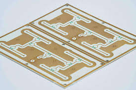
Large pcb prototype board
Advantages Of Using Large PCB Prototype Boards In Electronics Design
In the realm of electronics design, the use of large PCB (Printed Circuit Board) prototype boards has become increasingly prevalent, offering a multitude of advantages that significantly enhance the design and development process. As the demand for more complex and sophisticated electronic devices grows, the need for efficient and effective prototyping solutions becomes paramount. Large PCB prototype boards provide a versatile platform that accommodates intricate designs, allowing engineers to experiment and iterate with greater flexibility.
One of the primary advantages of using large PCB prototype boards is the ample space they offer for component placement and routing.
This increased real estate is particularly beneficial when dealing with complex circuits that require numerous components and intricate connections. By providing more room, large prototype boards enable designers to lay out components in a manner that optimizes performance and minimizes interference, which is crucial for maintaining signal integrity and reducing electromagnetic interference. Consequently, this leads to more reliable and efficient electronic devices.
Moreover, large PCB prototype boards facilitate the integration of multiple functionalities onto a single board.
This capability is especially advantageous in the development of multifunctional devices, where space constraints can often pose significant challenges. By utilizing a larger board, designers can incorporate various subsystems and components without the need for multiple smaller boards, thereby streamlining the design process and reducing the complexity of interconnections. This not only simplifies the assembly process but also enhances the overall reliability of the final product.
In addition to accommodating complex designs, large PCB prototype boards also offer the advantage of scalability.
As projects evolve and requirements change, the ability to scale up the design without the need for a complete redesign is invaluable. Large boards provide the flexibility to add or modify components and circuits as needed, allowing for seamless adaptation to new specifications or technological advancements. This scalability is particularly beneficial in industries where rapid innovation is essential, such as consumer electronics and telecommunications.
Furthermore, the use of large PCB prototype boards can lead to cost savings in the long run.
While the initial cost of a larger board may be higher than that of a smaller one, the potential for reduced development time and fewer iterations can offset this expense. By enabling more comprehensive testing and validation during the prototyping phase, large boards help identify and rectify design flaws early in the process, thereby minimizing costly revisions and rework. This efficiency not only accelerates time-to-market but also enhances the overall cost-effectiveness of the project.
Another noteworthy advantage of large PCB prototype boards is their ability to support advanced testing and debugging techniques.
With more space available, designers can incorporate test points, diagnostic circuits, and other features that facilitate thorough testing and troubleshooting. This capability is crucial for ensuring the functionality and reliability of the final product, as it allows for the identification and resolution of potential issues before mass production.
In conclusion, the use of large PCB prototype boards in electronics design offers a range of benefits that contribute to more efficient, reliable, and cost-effective development processes. By providing ample space for complex designs, enabling scalability, and supporting advanced testing methods, these boards play a pivotal role in meeting the demands of modern electronic devices. As technology continues to advance, the importance of large PCB prototype boards in facilitating innovation and excellence in electronics design is likely to grow even further.
Key Considerations When Designing Large PCB Prototype Boards
When designing large PCB prototype boards, several key considerations must be taken into account to ensure both functionality and manufacturability. The complexity of these boards often demands a meticulous approach, as they serve as the foundation for electronic devices that require precise and reliable performance. To begin with, one of the primary considerations is the layout design. The layout must be carefully planned to accommodate the various components and connections, ensuring that signal integrity is maintained throughout the board. This involves strategic placement of components to minimize signal path lengths and reduce potential interference, which is crucial for maintaining the board’s overall performance.
In addition to layout design, the choice of materials plays a significant role in the success of a large PCB prototype board.
The substrate material must be selected based on the specific requirements of the application, such as thermal conductivity, dielectric constant, and mechanical strength. For instance, high-frequency applications may require materials with low dielectric loss to ensure signal integrity, while boards that will be subjected to harsh environments might need substrates with enhanced thermal and mechanical properties. Therefore, understanding the operational environment and performance requirements is essential when selecting materials.
Another critical aspect to consider is the power distribution network (PDN).
As the size of the PCB increases, so does the complexity of the PDN. It is vital to design a robust PDN that can efficiently deliver power to all components without causing voltage drops or introducing noise. This often involves the use of multiple power and ground planes, as well as careful consideration of trace widths and via placements to ensure adequate current carrying capacity. Additionally, incorporating decoupling capacitors near power pins can help mitigate power fluctuations and maintain stable operation.
Thermal management is also a crucial factor in the design of large PCB prototype boards.
As electronic components become more densely packed, the risk of overheating increases, which can lead to performance degradation or even failure. Effective thermal management strategies, such as the use of heat sinks, thermal vias, and proper airflow design, must be implemented to dissipate heat efficiently. Moreover, thermal simulations can be conducted during the design phase to identify potential hotspots and optimize the board layout accordingly.
Signal integrity is another important consideration, particularly for high-speed applications.
As signal frequencies increase, issues such as crosstalk, reflection, and electromagnetic interference (EMI) become more pronounced. To address these challenges, designers must pay close attention to trace impedance, routing techniques, and the use of shielding or differential signaling where necessary. Additionally, conducting signal integrity simulations can help identify potential issues and guide design adjustments to ensure reliable signal transmission.
Finally, manufacturability should not be overlooked when designing large PCB prototype boards.
The design must be compatible with standard manufacturing processes to avoid unnecessary costs and delays. This includes adhering to design for manufacturability (DFM) guidelines, such as maintaining appropriate trace widths and spacing, ensuring proper hole sizes for vias, and considering panelization for efficient production. By keeping manufacturability in mind from the outset, designers can streamline the transition from prototype to production, ultimately reducing time-to-market and ensuring a successful product launch.
In conclusion, designing large PCB prototype boards requires a comprehensive approach that considers layout design, material selection, power distribution, thermal management, signal integrity, and manufacturability. By addressing these key considerations, designers can create robust and reliable boards that meet the demands of modern electronic applications.
Common Challenges And Solutions In Large PCB Prototype Board Fabrication
The fabrication of large PCB prototype boards presents a unique set of challenges that can significantly impact the efficiency and success of electronic product development. As the demand for more complex and high-performance electronic devices grows, engineers and manufacturers are increasingly tasked with overcoming these obstacles to deliver reliable and functional prototypes. Understanding the common challenges associated with large PCB prototype board fabrication and exploring potential solutions is crucial for optimizing the design and manufacturing process.
One of the primary challenges in fabricating large PCB prototype boards is maintaining signal integrity.
As the size of the board increases, so does the length of the traces, which can lead to signal degradation due to increased resistance, inductance, and capacitance. This can result in issues such as signal delay, crosstalk, and electromagnetic interference, all of which can compromise the performance of the final product. To address these issues, designers can employ techniques such as impedance matching, differential signaling, and the use of ground planes to minimize interference and maintain signal quality.
Another significant challenge is thermal management.
Large PCB prototype boards often house numerous components that generate heat, which can lead to overheating and potential failure if not properly managed. Effective thermal management strategies are essential to ensure the longevity and reliability of the board. Solutions include the use of thermal vias, heat sinks, and thermal interface materials to dissipate heat efficiently. Additionally, careful placement of components and the use of thermal simulation software during the design phase can help identify potential hotspots and optimize the thermal performance of the board.
The mechanical stability of large PCB prototype boards is also a concern, as they are more susceptible to warping and bending due to their size.
This can lead to mechanical stress on components and solder joints, potentially causing failures. To mitigate these risks, manufacturers can use thicker substrates or incorporate stiffeners to enhance the board’s rigidity. Furthermore, selecting materials with low coefficients of thermal expansion can help reduce the risk of warping during temperature fluctuations.
Manufacturing large PCB prototype boards also poses logistical challenges, particularly in terms of handling and transportation.
The sheer size of these boards can make them difficult to maneuver during the fabrication process, increasing the risk of damage. To address this, manufacturers can implement specialized handling equipment and procedures to ensure safe and efficient movement of the boards throughout the production line. Additionally, collaboration with logistics partners experienced in handling large and delicate items can help ensure that the boards are transported safely to their final destination.
Cost is another factor that cannot be overlooked when dealing with large PCB prototype boards.
The increased material usage, complexity, and potential for rework can drive up production costs significantly. To manage expenses, designers and manufacturers can focus on optimizing the design for manufacturability, which involves simplifying the design where possible and selecting cost-effective materials and processes. Engaging in early collaboration between design and manufacturing teams can also help identify potential cost-saving opportunities and streamline the production process.
In conclusion, while the fabrication of large PCB prototype boards presents several challenges, understanding these issues and implementing effective solutions can lead to successful outcomes. By focusing on signal integrity, thermal management, mechanical stability, logistical considerations, and cost optimization, engineers and manufacturers can overcome the obstacles associated with large PCB prototype board fabrication and deliver high-quality prototypes that meet the demands of modern electronic applications.
Innovations In Large PCB Prototype Board Technology And Their Impact On The Industry
The evolution of large PCB prototype board technology has been a cornerstone in the advancement of the electronics industry, driving innovation and efficiency across various sectors. As the demand for more complex and high-performance electronic devices continues to grow, the need for sophisticated and reliable PCB prototypes has become increasingly critical. This has led to significant innovations in the design, manufacturing, and testing of large PCB prototype boards, which are now more capable than ever of meeting the rigorous demands of modern electronics.
One of the most notable advancements in large PCB prototype board technology is the development of high-density interconnect (HDI) technology.
HDI boards are characterized by their finer lines and spaces, smaller vias, and higher connection pad density, which allow for more components to be placed on a single board. This innovation has enabled the creation of smaller, lighter, and more powerful electronic devices, which are essential in industries such as telecommunications, aerospace, and consumer electronics. The ability to integrate more functionality into a smaller footprint not only enhances device performance but also reduces manufacturing costs and time-to-market.
In addition to HDI technology, the use of advanced materials has also played a crucial role in the evolution of large PCB prototype boards.
Materials such as high-frequency laminates and flexible substrates have expanded the capabilities of PCBs, allowing them to operate efficiently in high-speed and high-frequency applications. These materials provide superior thermal management and signal integrity, which are vital for the performance and reliability of modern electronic devices. As a result, industries that rely on high-speed data transmission, such as data centers and automotive electronics, have greatly benefited from these material innovations.
Moreover, the integration of automated design and manufacturing processes has revolutionized the production of large PCB prototype boards.
Computer-aided design (CAD) software and automated assembly lines have significantly reduced the time and cost associated with PCB prototyping. These technologies enable precise and efficient design iterations, allowing engineers to quickly test and refine their prototypes. This agility is particularly important in today’s fast-paced market, where the ability to rapidly develop and deploy new products can be a decisive competitive advantage.
Furthermore, the implementation of advanced testing and quality assurance methods has ensured that large PCB prototype boards meet the highest standards of performance and reliability.
Techniques such as automated optical inspection (AOI) and X-ray inspection have become integral to the prototyping process, allowing for the early detection of defects and ensuring that only the highest quality boards reach the market. This focus on quality not only enhances the reputation of manufacturers but also instills confidence in end-users who rely on these critical components.
In conclusion, the innovations in large PCB prototype board technology have had a profound impact on the electronics industry, enabling the development of more advanced, efficient, and reliable electronic devices. The advancements in HDI technology, materials, automated processes, and testing methods have collectively transformed the way PCBs are designed and manufactured. As the industry continues to evolve, these innovations will undoubtedly play a pivotal role in shaping the future of electronics, driving further advancements and opening new possibilities for technological growth.