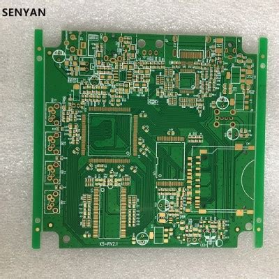
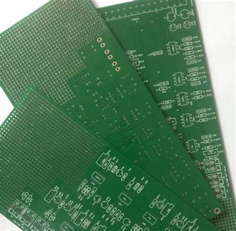
Large pcb manufacturing
Advantages Of Using Large PCB Prototype Boards In Complex Circuit Designs
In the realm of electronics and circuit design, the use of large PCB (Printed Circuit Board) prototype boards has become increasingly prevalent, particularly in the development of complex circuit designs. These boards offer a multitude of advantages that facilitate the design, testing, and refinement of intricate electronic systems. As technology continues to advance, the demand for more sophisticated and multifaceted electronic devices grows, making the role of large PCB prototype boards ever more critical.
One of the primary advantages of using large PCB prototype boards is the ample space they provide for accommodating complex circuit layouts.
In intricate designs, where numerous components and connections are involved, having sufficient space is crucial. Large prototype boards allow designers to spread out components, reducing the risk of overcrowding and minimizing the potential for errors during the assembly process. This spaciousness not only aids in the organization of components but also enhances the overall reliability of the circuit by reducing the likelihood of short circuits and other malfunctions.
Moreover, large PCB prototype boards offer enhanced flexibility in design modifications and iterations.
During the development phase, it is common for engineers to make adjustments to the circuit design to optimize performance or address unforeseen issues. With a larger board, there is more room to experiment with different configurations and to add or remove components as needed. This flexibility is particularly beneficial in the prototyping stage, where rapid iterations are often necessary to refine the design before final production.
In addition to providing ample space and flexibility, large PCB prototype boards also facilitate improved thermal management.
Complex circuits often generate significant amounts of heat, which can adversely affect performance and longevity if not properly managed. Larger boards allow for better heat dissipation, as there is more surface area available to distribute heat away from critical components. This can be further enhanced by incorporating thermal vias and heat sinks, which are more easily accommodated on a larger board. Effective thermal management is essential in maintaining the stability and efficiency of complex electronic systems.
Furthermore, large PCB prototype boards enable more comprehensive testing and troubleshooting.
With more space available, engineers can incorporate additional test points and diagnostic features into the design. This allows for more thorough testing of the circuit’s functionality and performance, making it easier to identify and rectify any issues that may arise. The ability to conduct extensive testing is invaluable in ensuring that the final product meets the desired specifications and operates reliably under various conditions.
Another significant advantage of using large PCB prototype boards is the potential for integrating advanced features and technologies.
As electronic devices become more sophisticated, there is an increasing need to incorporate features such as wireless connectivity, advanced sensors, and complex processing capabilities. Large boards provide the necessary real estate to integrate these advanced components without compromising the design’s integrity or functionality. This capability is crucial in keeping pace with technological advancements and meeting the evolving demands of consumers and industries alike.
In conclusion, the use of large PCB prototype boards in complex circuit designs offers numerous advantages that enhance the design, testing, and refinement processes. By providing ample space, flexibility, improved thermal management, comprehensive testing capabilities, and the potential for advanced feature integration, these boards play a vital role in the development of sophisticated electronic systems. As technology continues to evolve, the importance of large PCB prototype boards in facilitating innovation and ensuring the reliability of complex circuits will undoubtedly continue to grow.
Key Considerations When Designing Large PCB Prototype Boards
When designing large PCB prototype boards, several key considerations must be taken into account to ensure the successful development and functionality of the final product. The complexity of large PCBs demands meticulous planning and attention to detail, as these boards often serve as the backbone for sophisticated electronic systems.
One of the primary considerations is the layout design, which plays a crucial role in the performance and reliability of the PCB.
A well-thought-out layout can minimize issues such as signal interference and power distribution problems, which are more prevalent in larger boards due to the increased number of components and longer trace lengths.
Transitioning from layout design, another critical factor is the selection of materials.
The choice of substrate material can significantly impact the thermal and electrical performance of the PCB. For large boards, materials with excellent thermal conductivity and low dielectric loss are preferred to ensure efficient heat dissipation and signal integrity. Additionally, the thickness of the board must be considered, as it affects both the mechanical stability and the impedance of the traces. Designers must strike a balance between these factors to optimize the board’s performance.
Furthermore, the complexity of large PCB prototype boards necessitates careful consideration of the power distribution network.
Ensuring that power is delivered efficiently to all components is vital to prevent voltage drops and power integrity issues. This involves designing a robust power distribution network with adequate power planes and decoupling capacitors strategically placed to minimize noise and ensure stable operation. The use of simulation tools can aid in predicting and mitigating potential power distribution problems before the board is fabricated.
In addition to power distribution, signal integrity is another paramount consideration.
As the size of the PCB increases, so does the potential for signal degradation due to factors such as crosstalk, reflection, and electromagnetic interference. To address these challenges, designers must carefully route high-speed signals, paying attention to trace impedance and length matching. Implementing differential signaling and shielding techniques can also help maintain signal integrity across the board.
Moreover, thermal management is a critical aspect that cannot be overlooked when designing large PCB prototype boards.
The increased component density and power consumption can lead to significant heat generation, which, if not managed properly, can affect the performance and lifespan of the board. Effective thermal management strategies, such as the use of heat sinks, thermal vias, and proper airflow design, are essential to dissipate heat efficiently and maintain optimal operating temperatures.
Transitioning to the manufacturing process, designers must also consider the manufacturability of large PCB prototype boards.
The complexity and size of these boards can pose challenges during fabrication, such as difficulties in achieving precise alignment and registration. Collaborating closely with manufacturers during the design phase can help identify potential issues and ensure that the board can be produced reliably and cost-effectively.
Finally, testing and validation are crucial steps in the design process of large PCB prototype boards. Comprehensive testing ensures that the board meets all design specifications and functions as intended. This includes electrical testing to verify connectivity and performance, as well as environmental testing to assess the board’s resilience under various conditions. By addressing these key considerations, designers can create large PCB prototype boards that are not only functional but also reliable and efficient, paving the way for successful electronic systems.
Cost-Effective Strategies For Manufacturing Large PCB Prototype Boards
When it comes to manufacturing large PCB prototype boards, cost-effectiveness is a crucial consideration for businesses aiming to optimize their production processes. The development of these boards, which serve as the foundation for electronic devices, involves several intricate steps that can significantly impact the overall budget. Therefore, understanding and implementing cost-effective strategies is essential for companies seeking to maintain competitive pricing while ensuring high-quality outcomes.
To begin with, selecting the right materials is a fundamental step in reducing costs.
The choice of substrate material, such as FR-4, polyimide, or metal-core, can influence both the performance and the expense of the PCB. While high-performance materials may offer superior thermal and electrical properties, they often come at a premium. Thus, it is important to balance performance requirements with budget constraints. By carefully evaluating the specific needs of the project, manufacturers can choose materials that provide adequate functionality without unnecessary expenditure.
In addition to material selection, optimizing the design layout is another effective strategy for cost reduction.
A well-thought-out design can minimize the number of layers required, thereby reducing material costs and manufacturing complexity. Employing design for manufacturability (DFM) principles can help identify potential issues early in the design phase, allowing for adjustments that streamline production. For instance, ensuring that the design adheres to standard panel sizes can minimize waste and improve yield, ultimately lowering costs.
Furthermore, leveraging advanced software tools for simulation and testing can significantly enhance the efficiency of the prototyping process.
These tools allow designers to identify and rectify potential issues before physical production begins, reducing the likelihood of costly revisions. By simulating the electrical and thermal performance of the PCB, manufacturers can ensure that the design meets all necessary specifications, thereby avoiding expensive rework and delays.
Another cost-effective approach involves collaborating with experienced PCB manufacturers who offer prototyping services.
These partners often possess the expertise and resources to optimize production processes, resulting in cost savings. By outsourcing the prototyping phase to a specialized provider, companies can benefit from economies of scale and access to advanced manufacturing technologies without the need for significant capital investment.
Moreover, considering the use of panelization techniques can further enhance cost efficiency.
Panelization involves grouping multiple PCB designs onto a single panel, allowing for simultaneous production. This approach not only reduces material waste but also decreases production time and costs. By maximizing the use of available space on each panel, manufacturers can achieve higher throughput and lower per-unit costs.
Finally, maintaining open communication with suppliers and manufacturers is vital for identifying potential cost-saving opportunities.
By establishing strong relationships and engaging in regular discussions, companies can gain insights into market trends, material availability, and pricing fluctuations. This proactive approach enables businesses to make informed decisions and negotiate favorable terms, ultimately contributing to a more cost-effective manufacturing process.
In conclusion, manufacturing large PCB prototype boards in a cost-effective manner requires a multifaceted approach that encompasses material selection, design optimization, advanced simulation tools, strategic partnerships, and efficient production techniques. By carefully considering each of these elements and implementing best practices, companies can achieve significant cost savings while maintaining the quality and performance of their PCB prototypes. This strategic focus not only enhances competitiveness but also positions businesses for long-term success in the ever-evolving electronics industry.
Common Challenges And Solutions In Large PCB Prototype Board Development
Developing large PCB prototype boards presents a unique set of challenges that can significantly impact the efficiency and success of electronic projects. As the demand for more complex and powerful electronic devices grows, engineers and designers are increasingly tasked with creating larger and more intricate printed circuit boards (PCBs). These boards serve as the backbone of electronic devices, providing the necessary pathways for electrical signals to travel between components. However, the development of large PCB prototypes is fraught with potential difficulties that require careful consideration and strategic solutions.
One of the primary challenges in large PCB prototype board development is managing the increased complexity that comes with a larger board size.
As the board size increases, so does the number of components and connections, which can lead to a more complicated design process. This complexity can result in longer design times and a higher likelihood of errors. To address this issue, designers can utilize advanced PCB design software that offers features such as automated routing and design rule checks. These tools can help streamline the design process and reduce the risk of errors by ensuring that all connections are correctly made and that the board adheres to industry standards.
Another significant challenge is maintaining signal integrity across the larger board area.
As the size of the PCB increases, so does the potential for signal degradation due to longer trace lengths and increased electromagnetic interference (EMI). To mitigate these issues, designers can employ techniques such as differential signaling, controlled impedance routing, and the use of ground planes. These methods help to maintain signal quality by minimizing interference and ensuring that signals are transmitted efficiently across the board.
Thermal management is also a critical concern in the development of large PCB prototype boards.
Larger boards often house more components, which can generate significant amounts of heat. If not properly managed, this heat can lead to component failure and reduced board performance. To address thermal management challenges, designers can incorporate heat sinks, thermal vias, and copper pours into their designs. Additionally, conducting thermal simulations during the design phase can help identify potential hotspots and allow for proactive measures to be taken.
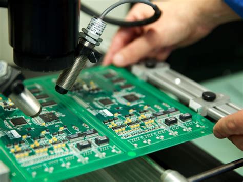
Furthermore, the manufacturing process for large PCB prototypes can present its own set of challenges.
Larger boards may require specialized equipment and processes, which can increase production costs and lead times. To overcome these obstacles, it is essential to work closely with experienced PCB manufacturers who have the capability to handle large-scale production. Collaborating with manufacturers early in the design process can also help identify potential manufacturing issues and allow for design adjustments that facilitate smoother production.
Finally, testing and validation of large PCB prototypes can be more complex and time-consuming than for smaller boards.
The increased number of components and connections requires more extensive testing to ensure that the board functions as intended. Implementing a comprehensive testing strategy that includes both automated and manual testing methods can help identify and address any issues before the board goes into full production.
In conclusion, while the development of large PCB prototype boards presents several challenges, these can be effectively managed through careful planning, the use of advanced design tools, and collaboration with experienced manufacturers. By addressing complexity, signal integrity, thermal management, manufacturing, and testing challenges, designers can successfully develop large PCB prototypes that meet the demands of modern electronic devices.