Kicad multilayer pcb
Designing Multilayer PCBs with KiCad: A Step-by-Step Guide
Designing multilayer printed circuit boards (PCBs) is a complex yet rewarding task that requires a deep understanding of both the software tools and the principles of electronics design. KiCad, an open-source PCB design software, has become increasingly popular among engineers and hobbyists alike due to its robust features and cost-effectiveness. This guide aims to provide a comprehensive overview of the process involved in designing multilayer PCBs using KiCad, ensuring that even those new to the software can follow along with ease.
To begin with, it is essential to understand the advantages of using multilayer PCBs.
These boards allow for more complex and compact designs by providing additional layers for routing signals, power, and ground planes. This not only enhances the electrical performance of the circuit but also reduces electromagnetic interference. As a result, multilayer PCBs are widely used in advanced electronics applications, including telecommunications, aerospace, and consumer electronics.
The first step in designing a multilayer PCB with KiCad is to create a schematic diagram.
This involves placing and connecting electronic components to define the circuit’s functionality. KiCad’s schematic editor is intuitive and offers a vast library of components, making it easier to find and place the necessary parts. Once the schematic is complete, it is crucial to run an electrical rules check to ensure there are no errors or unconnected nets.
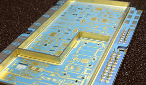
Following the schematic design, the next phase is to define the board’s stack-up.
This involves specifying the number of layers and their respective functions, such as signal, power, or ground layers. KiCad allows users to customize the stack-up according to their design requirements, providing flexibility in layer arrangement and thickness. It is important to consider factors such as signal integrity and thermal management when configuring the stack-up, as these can significantly impact the board’s performance.
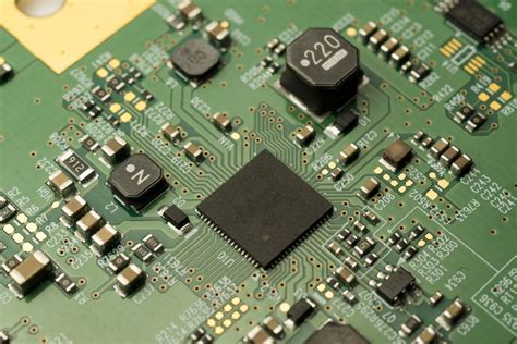
With the stack-up defined, the layout process begins.
This involves placing components on the board and routing the connections between them. KiCad’s PCB editor offers powerful tools for component placement and track routing, including interactive routing and design rule checks. These features help ensure that the layout adheres to the specified design rules, such as minimum trace width and clearance, which are critical for maintaining signal integrity and manufacturability.
As the design progresses, it is essential to continuously verify the layout against the schematic to prevent discrepancies.
KiCad provides a netlist comparison tool that highlights any mismatches between the schematic and PCB layout, allowing designers to address issues promptly. Additionally, performing a design rule check at various stages of the layout process can help identify potential violations early, reducing the risk of costly errors in the final design.
Once the layout is complete, the final step is to generate the necessary files for manufacturing.
KiCad supports the export of Gerber files, which are the industry standard for PCB fabrication. These files contain all the information required by manufacturers to produce the board, including layer data, drill files, and assembly drawings. It is advisable to review these files thoroughly before submission to ensure accuracy and completeness.
In conclusion, designing multilayer PCBs with KiCad involves a series of well-defined steps, from schematic creation to layout and file generation. By leveraging KiCad’s powerful features and adhering to best practices, designers can create high-quality multilayer PCBs that meet their specific requirements. As technology continues to advance, mastering tools like KiCad will be invaluable for those looking to innovate in the field of electronics design.
Optimizing Signal Integrity in KiCad Multilayer PCB Designs
In the realm of electronic design, optimizing signal integrity is a critical aspect that can significantly influence the performance and reliability of a printed circuit board (PCB). KiCad, an open-source PCB design tool, offers a robust platform for creating multilayer PCBs, which are essential for complex electronic systems. Multilayer PCBs provide the necessary infrastructure to manage high-speed signals, reduce electromagnetic interference, and improve overall circuit performance. To achieve optimal signal integrity in KiCad multilayer PCB designs, several key considerations must be addressed.
Firstly, understanding the stack-up configuration is fundamental.
The stack-up refers to the arrangement of conductive and insulating layers within the PCB. A well-planned stack-up can minimize signal loss and crosstalk, which are common issues in high-speed circuits. Typically, a multilayer PCB will include power and ground planes, which serve as reference planes for signal layers. By strategically placing these planes, designers can create controlled impedance environments that are crucial for maintaining signal integrity. In KiCad, users can define the stack-up in the PCB Editor, allowing for precise control over layer arrangements and material properties.
Moreover, trace routing plays a pivotal role in signal integrity.
In multilayer designs, traces should be routed to minimize their length and avoid sharp angles, which can cause signal reflections and degrade performance. KiCad provides various routing tools that facilitate the creation of efficient trace paths. For instance, the differential pair routing feature is particularly useful for high-speed signals, ensuring that paired traces maintain consistent spacing and length. Additionally, employing via stitching can help reduce loop areas and improve return path continuity, further enhancing signal integrity.
Transitioning to the topic of grounding, a solid grounding strategy is indispensable for mitigating noise and ensuring stable operation.
In multilayer PCBs, ground planes act as a shield against electromagnetic interference and provide a low-impedance path for return currents. KiCad allows designers to define dedicated ground layers, which can be connected to components and traces using vias. It is advisable to maintain a continuous ground plane across the PCB to prevent ground loops and potential signal integrity issues.
Furthermore, power distribution is another critical aspect that influences signal integrity.
Proper power plane design can reduce voltage drops and minimize power supply noise, which are detrimental to high-speed circuits. In KiCad, power planes can be defined similarly to ground planes, and careful attention should be paid to their layout to ensure even power distribution. Decoupling capacitors should be strategically placed near power pins to filter out high-frequency noise and stabilize the power supply.
In addition to these technical considerations, simulation and analysis are invaluable tools for optimizing signal integrity.
KiCad integrates with various simulation software, enabling designers to model and analyze their PCB designs before fabrication. By simulating signal behavior, designers can identify potential issues and make necessary adjustments to improve performance.
In conclusion, optimizing signal integrity in KiCad multilayer PCB designs requires a comprehensive approach that encompasses stack-up configuration, trace routing, grounding, power distribution, and simulation. By leveraging the capabilities of KiCad and adhering to best practices, designers can create high-performance PCBs that meet the demands of modern electronic applications. As technology continues to advance, the importance of signal integrity in PCB design will only grow, making it essential for designers to stay informed and adept in their design practices.
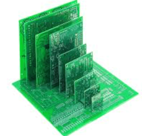
Best Practices for Layer Stackup in KiCad Multilayer PCBs
Designing multilayer printed circuit boards (PCBs) in KiCad requires a comprehensive understanding of layer stackup, which is crucial for ensuring optimal performance and reliability. A well-considered layer stackup not only enhances the electrical performance of the PCB but also aids in thermal management and mechanical stability. To achieve these objectives, it is essential to follow best practices that guide the arrangement and utilization of layers in a multilayer PCB design.
Firstly, it is important to determine the number of layers required for your design.
This decision is influenced by factors such as the complexity of the circuit, the density of components, and the need for controlled impedance. Typically, a four-layer stackup is a common starting point for many designs, offering two signal layers and two planes for power and ground. However, more complex designs may necessitate additional layers to accommodate intricate routing and to maintain signal integrity.
Once the number of layers is established, the next step is to define the purpose of each layer.
Generally, the outermost layers are used for signal routing, while the inner layers are designated for power and ground planes. This configuration helps in minimizing electromagnetic interference (EMI) and crosstalk by providing a continuous return path for signals. Moreover, placing power and ground planes adjacent to each other can create a high-frequency decoupling effect, which is beneficial for reducing noise.
In addition to layer assignment, the thickness of each layer plays a significant role in the overall performance of the PCB.
The dielectric material between layers should be chosen carefully to ensure the desired impedance and to support the mechanical strength of the board. It is advisable to consult with your PCB manufacturer to understand the available material options and their properties, as this can impact both the electrical performance and the cost of the PCB.
Furthermore, attention must be paid to the routing of high-speed signals.
These signals should be routed on layers adjacent to a ground plane to minimize impedance discontinuities and to provide a clear return path. Differential pairs, commonly used in high-speed designs, should be routed symmetrically and with consistent spacing to maintain their characteristic impedance. Additionally, vias should be used judiciously, as excessive use can introduce parasitic inductance and capacitance, potentially degrading signal integrity.
Thermal management is another critical aspect of multilayer PCB design.
The layer stackup should facilitate efficient heat dissipation, especially in high-power applications. Incorporating thermal vias and copper pours can help in spreading heat across the board, thereby preventing hotspots and ensuring the longevity of components.
Finally, it is essential to validate the layer stackup through simulation and analysis before proceeding to fabrication.
Tools within KiCad, as well as third-party simulation software, can be used to model the electrical and thermal behavior of the PCB. This step is crucial for identifying potential issues and making necessary adjustments to the design.
In conclusion, designing a multilayer PCB in KiCad involves careful consideration of layer stackup to achieve optimal performance. By determining the appropriate number of layers, defining their purpose, selecting suitable materials, and adhering to best practices for routing and thermal management, designers can create reliable and efficient PCBs. Through diligent planning and validation, the complexities of multilayer PCB design can be effectively managed, resulting in a successful final product.
Troubleshooting Common Issues in KiCad Multilayer PCB Projects
Designing multilayer printed circuit boards (PCBs) using KiCad can be a rewarding endeavor, offering the ability to create complex and compact electronic circuits. However, as with any sophisticated design process, it is not uncommon to encounter various challenges. Understanding these common issues and knowing how to troubleshoot them can significantly enhance the efficiency and success of your projects.
One frequent issue in multilayer PCB design is the misalignment of layers.
This can occur due to discrepancies in the design files or errors during the manufacturing process. To mitigate this, it is crucial to ensure that all layers are correctly aligned in the design phase. Utilizing KiCad’s layer alignment tools can help maintain precision. Additionally, conducting a thorough design rule check (DRC) before sending the files for fabrication can catch potential misalignments early.
Another common problem is the incorrect configuration of vias, which are essential for connecting different layers of a PCB.
Vias must be carefully designed to handle the required current and signal integrity. Inadequate via design can lead to issues such as signal loss or overheating. To address this, KiCad provides options to customize via sizes and types, such as through-hole or blind vias, according to the specific needs of your project. Ensuring that the vias are properly configured and placed can prevent these issues from arising.
Signal integrity is another critical aspect that can be problematic in multilayer PCB designs
High-speed signals, in particular, are susceptible to issues such as crosstalk and electromagnetic interference (EMI). To troubleshoot these problems, it is advisable to use KiCad’s simulation tools to analyze signal paths and identify potential sources of interference. Implementing strategies such as proper trace routing, maintaining adequate spacing between traces, and using ground planes effectively can help mitigate signal integrity issues.
Thermal management is also a significant concern in multilayer PCB projects.
The compact nature of these designs can lead to heat accumulation, which can affect the performance and longevity of the components. To address thermal issues, it is important to consider the thermal properties of the materials used and incorporate thermal vias and heat sinks where necessary. KiCad allows designers to simulate thermal behavior, providing insights into potential hotspots and enabling proactive design adjustments.
Component placement is another area where challenges may arise. In multilayer designs, the placement of components can significantly impact the overall functionality and manufacturability of the PCB.
Poor component placement can lead to difficulties in routing and increased susceptibility to noise. To optimize component placement, it is beneficial to follow best practices such as grouping related components together and minimizing the length of critical signal paths. KiCad’s interactive placement tools can assist in achieving an efficient layout.
Finally, documentation errors can lead to misunderstandings and manufacturing defects.
Ensuring that all design files, including schematics, layout, and bill of materials (BOM), are accurate and up-to-date is essential. KiCad offers features to generate comprehensive documentation, which can be invaluable for both the design and manufacturing stages.
In conclusion, while designing multilayer PCBs in KiCad presents certain challenges, understanding and addressing these common issues can lead to successful project outcomes. By leveraging KiCad’s robust set of tools and adhering to best practices, designers can effectively troubleshoot and overcome the obstacles inherent in multilayer PCB design.