Jablotron pcb assembly
Understanding The Basics Of Jablotron PCB Assembly
Jablotron, a renowned name in the field of electronic security systems, has made significant strides in the development and assembly of printed circuit boards (PCBs). Understanding the basics of Jablotron PCB assembly is crucial for those interested in the intricacies of electronic manufacturing and design. At the heart of any electronic device, PCBs serve as the foundation upon which all electronic components are mounted and interconnected. The assembly process involves several meticulous steps, each contributing to the overall functionality and reliability of the final product.
Initially, the design phase is paramount, as it sets the blueprint for the entire assembly process.
Engineers utilize sophisticated software to create detailed schematics and layouts, ensuring that the PCB will meet the specific requirements of the intended application. This stage involves careful consideration of component placement, signal routing, and thermal management, all of which are critical to the board’s performance. Once the design is finalized, it is translated into a set of manufacturing instructions that guide the subsequent stages of assembly.
Following the design phase, the focus shifts to the fabrication of the PCB itself.
This involves the creation of the board’s physical structure, typically composed of multiple layers of conductive and insulating materials. The fabrication process includes etching, drilling, and plating, which collectively form the intricate network of pathways that facilitate electrical connections between components. Precision is essential during this stage, as any deviation from the design specifications can lead to functional issues or even complete failure of the board.
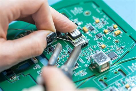
Once the PCB is fabricated, the assembly process begins with the placement of components onto the board.
This step is often automated, utilizing advanced machinery to position components with remarkable accuracy and speed. Surface mount technology (SMT) is commonly employed, allowing for the efficient placement of small, lightweight components directly onto the board’s surface. This method not only enhances the board’s performance but also reduces its overall size and weight, which is particularly advantageous in compact electronic devices.
After component placement, the next critical step is soldering, which secures the components to the board and establishes electrical connections.
Reflow soldering is a widely used technique in which the entire board is heated in a controlled environment, causing the solder to melt and form strong bonds between the components and the PCB. This process requires precise temperature control to prevent damage to sensitive components while ensuring reliable connections.
Quality control is an integral part of the Jablotron PCB assembly process, ensuring that each board meets stringent standards before it is integrated into a final product.
Automated optical inspection (AOI) and X-ray inspection are commonly used to detect any defects or inconsistencies, such as misaligned components or incomplete solder joints. These advanced inspection techniques help maintain the high level of quality and reliability that Jablotron is known for.
In conclusion, understanding the basics of Jablotron PCB assembly provides valuable insight into the complex processes involved in creating reliable and efficient electronic devices. From the initial design phase to the final quality control checks, each step plays a crucial role in ensuring that the finished product meets the high standards expected in today’s competitive market. As technology continues to evolve, the methods and techniques used in PCB assembly will undoubtedly advance, further enhancing the capabilities and applications of electronic devices.

Key Challenges In Jablotron PCB Assembly And How To Overcome Them
In the realm of electronics manufacturing, the assembly of printed circuit boards (PCBs) is a critical process that demands precision and expertise. Jablotron, a renowned name in the security and automation industry, is no stranger to the complexities involved in PCB assembly. The process, while essential, is fraught with challenges that can impact the quality and functionality of the final product. Understanding these challenges and implementing strategies to overcome them is crucial for maintaining the high standards associated with Jablotron products.
One of the primary challenges in Jablotron PCB assembly is the miniaturization of components.
As technology advances, there is a growing demand for smaller, more compact devices. This trend necessitates the use of tiny components, which can be difficult to handle and place accurately on the PCB. To address this issue, manufacturers can invest in advanced pick-and-place machines that offer high precision and speed. Additionally, employing skilled technicians who are adept at working with small components can significantly reduce the risk of errors during assembly.
Another significant challenge is ensuring the reliability and durability of the solder joints.
Soldering is a critical step in PCB assembly, as it secures the components to the board and ensures electrical connectivity. Poor soldering can lead to weak joints, which may fail under stress or over time. To mitigate this risk, it is essential to use high-quality soldering materials and equipment. Moreover, implementing rigorous quality control measures, such as automated optical inspection (AOI) and X-ray inspection, can help identify and rectify soldering defects before the boards are finalized.
Thermal management is also a key concern in Jablotron PCB assembly.
As electronic devices become more powerful, they generate more heat, which can affect performance and longevity. Effective thermal management involves designing PCBs with adequate heat dissipation features, such as thermal vias and heat sinks. Additionally, selecting components with low thermal resistance and using thermal interface materials can enhance heat dissipation. By prioritizing thermal management during the design and assembly stages, manufacturers can ensure that Jablotron products operate efficiently and reliably.
Furthermore, the complexity of modern PCBs, with their multilayer designs and intricate circuitry, presents another challenge.
As PCBs become more complex, the risk of design errors increases, which can lead to costly rework or product failures. To overcome this challenge, it is vital to employ robust design verification and testing processes. Utilizing simulation software to test PCB designs before production can help identify potential issues early on. Additionally, conducting thorough testing at various stages of assembly can ensure that any defects are caught and corrected promptly.
Finally, supply chain management plays a crucial role in the success of Jablotron PCB assembly.
The availability and quality of components can significantly impact production timelines and product quality. To navigate this challenge, manufacturers should establish strong relationships with reliable suppliers and maintain a well-organized inventory system. By doing so, they can ensure a steady supply of high-quality components and minimize disruptions in the assembly process.
In conclusion, while Jablotron PCB assembly presents several challenges, they can be effectively managed through strategic planning and the implementation of advanced technologies. By focusing on precision, quality control, thermal management, design verification, and supply chain efficiency, manufacturers can overcome these obstacles and continue to deliver high-quality products that meet the expectations of Jablotron’s discerning customers.
Innovations In Jablotron PCB Assembly Technology
Jablotron, a renowned name in the field of electronic security systems, has consistently been at the forefront of technological innovation. One of the critical areas where Jablotron has demonstrated significant advancements is in printed circuit board (PCB) assembly technology. The evolution of PCB assembly processes has been instrumental in enhancing the performance, reliability, and efficiency of Jablotron’s products. As we delve into the innovations in Jablotron PCB assembly technology, it is essential to understand the broader context of PCB assembly and its impact on electronic devices.
To begin with, PCB assembly is a complex process that involves the integration of various electronic components onto a printed circuit board.
This process is crucial because it determines the functionality and durability of the final product. Jablotron has embraced cutting-edge technologies to refine this process, ensuring that their products meet the highest standards of quality and performance. One of the notable innovations in Jablotron’s PCB assembly is the adoption of surface mount technology (SMT). SMT allows for the placement of components directly onto the surface of the PCB, as opposed to the traditional through-hole method. This advancement not only reduces the size and weight of the boards but also enhances their performance by minimizing the distance that electrical signals must travel.
Moreover, Jablotron has integrated automated optical inspection (AOI) systems into their PCB assembly lines.
AOI systems are pivotal in ensuring the accuracy and precision of component placement. By using high-resolution cameras and sophisticated algorithms, these systems can detect even the slightest defects or misalignments, thereby significantly reducing the likelihood of errors. This level of precision is particularly important in security systems, where reliability is paramount.
In addition to SMT and AOI, Jablotron has also invested in advanced soldering techniques, such as reflow soldering.
Reflow soldering involves the application of solder paste to the PCB, followed by the controlled heating of the board to melt the solder and secure the components in place. This method is highly efficient and ensures strong, reliable connections between components and the PCB. The use of lead-free solder, in compliance with environmental regulations, further underscores Jablotron’s commitment to sustainability and safety.
Furthermore, Jablotron’s PCB assembly process benefits from the implementation of design for manufacturability (DFM) principles.
DFM involves designing PCBs in a way that simplifies the manufacturing process, reduces costs, and enhances product quality. By incorporating DFM principles, Jablotron can streamline production, minimize waste, and accelerate time-to-market for their products.
Another significant innovation in Jablotron’s PCB assembly technology is the use of flexible PCBs.
Unlike traditional rigid boards, flexible PCBs can be bent and shaped to fit into compact spaces, making them ideal for modern electronic devices that demand miniaturization without compromising functionality. This flexibility allows Jablotron to design more versatile and adaptable security systems that can meet the diverse needs of their customers.
In conclusion, the innovations in Jablotron PCB assembly technology reflect the company’s dedication to excellence and innovation. By leveraging advanced techniques such as surface mount technology, automated optical inspection, reflow soldering, and design for manufacturability, Jablotron continues to set new standards in the electronic security industry. These advancements not only enhance the performance and reliability of their products but also demonstrate a commitment to sustainability and customer satisfaction. As technology continues to evolve, Jablotron remains poised to lead the way in PCB assembly innovation, ensuring that their products remain at the cutting edge of security technology.
Best Practices For Quality Assurance In Jablotron PCB Assembly
In the realm of electronics manufacturing, ensuring the highest quality in printed circuit board (PCB) assembly is paramount, particularly for companies like Jablotron, which are renowned for their innovative security and automation solutions. Quality assurance in PCB assembly is a multifaceted process that requires meticulous attention to detail and adherence to best practices. By implementing a robust quality assurance framework, manufacturers can significantly enhance the reliability and performance of their products, thereby maintaining their competitive edge in the market.
To begin with, one of the fundamental best practices in quality assurance for Jablotron PCB assembly is the establishment of comprehensive design guidelines.
These guidelines serve as a blueprint for the entire assembly process, ensuring that each component is correctly placed and soldered. By adhering to these guidelines, manufacturers can minimize the risk of errors during assembly, which in turn reduces the likelihood of defects in the final product. Moreover, incorporating design for manufacturability (DFM) principles into the design phase can further streamline the assembly process, making it more efficient and less prone to errors.
In addition to design guidelines, rigorous testing procedures are essential for maintaining quality in PCB assembly.
Implementing a multi-tiered testing strategy, which includes in-circuit testing (ICT), functional testing, and automated optical inspection (AOI), can help identify and rectify defects at various stages of the assembly process. In-circuit testing allows for the verification of electrical connections and component functionality, while functional testing ensures that the assembled PCB performs as intended under real-world conditions. Automated optical inspection, on the other hand, provides a non-invasive method for detecting soldering defects and component misalignments, thereby enhancing the overall quality of the assembly.
Furthermore, the use of high-quality materials and components is crucial in ensuring the reliability of Jablotron PCB assemblies.
Sourcing components from reputable suppliers and maintaining stringent incoming quality control (IQC) procedures can prevent the introduction of substandard materials into the assembly process. By conducting thorough inspections and tests on incoming components, manufacturers can ensure that only those meeting the required specifications are used in the assembly, thereby reducing the risk of failures in the final product.
Another critical aspect of quality assurance in PCB assembly is the implementation of process control measures.
By employing statistical process control (SPC) techniques, manufacturers can monitor and control the assembly process in real-time, allowing for the early detection of deviations from established quality standards. This proactive approach enables manufacturers to address potential issues before they escalate, thereby maintaining the integrity of the assembly process and ensuring consistent product quality.
Moreover, continuous improvement is a cornerstone of effective quality assurance in PCB assembly.
By fostering a culture of continuous improvement, manufacturers can encourage their teams to identify and implement enhancements to the assembly process. This can be achieved through regular training sessions, feedback loops, and the adoption of industry best practices. By continuously refining their processes, manufacturers can not only improve product quality but also increase operational efficiency and reduce costs.
In conclusion, quality assurance in Jablotron PCB assembly is a complex yet essential endeavor that requires a holistic approach encompassing design, testing, materials, process control, and continuous improvement. By adhering to these best practices, manufacturers can ensure the production of high-quality PCBs that meet the stringent demands of the market, thereby reinforcing their reputation for excellence and innovation.