How to use prototype pcb
Understanding The Basics Of Prototype PCB Design
Prototype printed circuit boards (PCBs) serve as a crucial step in the development of electronic devices, allowing engineers and designers to test and refine their designs before mass production. Understanding the basics of prototype PCB design is essential for anyone involved in electronics development, as it lays the foundation for creating functional and efficient circuits.
To begin with, it is important to recognize that prototype PCBs are essentially a preliminary version of the final product, used to validate the design and functionality of the circuit. This process involves several key steps, each of which plays a vital role in ensuring the success of the final product.
Initially, the design process begins with the creation of a schematic diagram, which serves as a blueprint for the circuit.
This diagram outlines the components and their connections, providing a clear visual representation of the circuit’s intended functionality. It is crucial to ensure that the schematic is accurate and complete, as any errors at this stage can lead to significant issues later in the process. Once the schematic is finalized, the next step involves translating it into a layout design. This involves arranging the components on the PCB and routing the electrical connections between them. The layout design must take into account various factors, such as component placement, signal integrity, and thermal management, to ensure optimal performance.
As the layout design progresses, it is essential to consider the choice of materials and manufacturing processes.
The selection of materials can significantly impact the performance and reliability of the PCB, as well as its cost. Common materials used in prototype PCBs include FR-4, a fiberglass-reinforced epoxy laminate, and various types of copper for the conductive traces. Additionally, the manufacturing process must be carefully chosen to ensure that the prototype meets the desired specifications and tolerances. Techniques such as photolithography, etching, and solder mask application are commonly used in the production of prototype PCBs.
Once the prototype PCB is manufactured, the next step involves assembling the components onto the board.
This process, known as PCB assembly, requires precision and attention to detail to ensure that each component is correctly placed and soldered. It is important to follow the assembly guidelines provided by the component manufacturers, as improper assembly can lead to issues such as poor electrical connections or component damage. After assembly, the prototype PCB undergoes a series of tests to verify its functionality and performance. These tests may include electrical testing, thermal analysis, and signal integrity testing, among others. The results of these tests provide valuable feedback, allowing designers to identify and address any issues before proceeding to mass production.
In conclusion, understanding the basics of prototype PCB design is essential for anyone involved in electronics development.
By following a structured design process, from schematic creation to testing, designers can ensure that their prototype PCBs meet the desired specifications and function as intended. This not only helps to identify and resolve potential issues early in the development process but also paves the way for successful mass production. As technology continues to advance, the importance of prototype PCBs in the development of electronic devices will only continue to grow, making it imperative for designers to master the fundamentals of this critical process.
Step-By-Step Guide To Assembling Your Prototype PCB
Assembling a prototype printed circuit board (PCB) is a crucial step in the development of electronic devices, allowing engineers and hobbyists to test and refine their designs before mass production. To ensure a successful assembly, it is essential to follow a systematic approach, beginning with the preparation of necessary materials and tools. First, gather all components required for your PCB, including resistors, capacitors, integrated circuits, and any other specific parts outlined in your schematic. Additionally, ensure you have access to essential tools such as a soldering iron, solder wire, tweezers, and a multimeter for testing.
Once you have assembled your materials, the next step involves preparing the PCB itself.
Begin by inspecting the board for any visible defects or irregularities that could affect performance. It is advisable to clean the board using isopropyl alcohol to remove any contaminants that may have accumulated during manufacturing or handling. This step is crucial as it ensures optimal solder adhesion and prevents potential short circuits.
With the board prepared, the next phase involves placing the components onto the PCB.
Start by identifying the correct orientation and position for each component, referring to the design schematic and the silkscreen markings on the board. It is often beneficial to begin with the smallest components, such as resistors and capacitors, as they are easier to place and solder without interference from larger parts. Use tweezers to carefully position each component, ensuring that the leads align with the corresponding holes on the PCB.
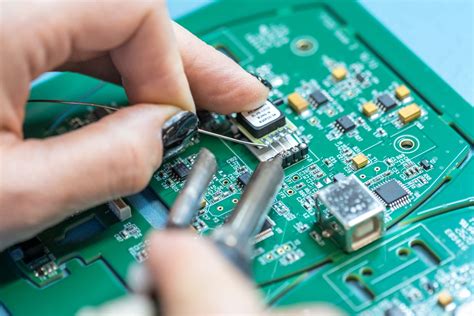
Following the placement of components, the soldering process begins.
Preheat your soldering iron to the appropriate temperature, typically around 350°C for most lead-based solders. Apply a small amount of solder to the tip of the iron to improve heat transfer, then proceed to solder each component in place. It is important to apply the solder to the joint where the component lead meets the PCB pad, allowing the heat to draw the solder into a secure connection. Take care to avoid excessive solder, which can lead to bridging between adjacent pads and cause short circuits.
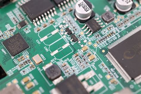
After soldering all components, it is prudent to inspect each joint for quality and reliability.
A good solder joint should appear shiny and smooth, with a concave shape that indicates proper wetting of the pad and lead. If any joints appear dull or irregular, reheat and apply additional solder as necessary. Once satisfied with the soldering, trim any excess leads protruding from the board using flush cutters.
The final step in assembling your prototype PCB involves testing the assembled board to ensure functionality.
Use a multimeter to check for continuity between connected pads and verify that there are no unintended short circuits. Power the board and conduct functional tests according to your design specifications, observing for any anomalies or malfunctions. If issues arise, systematically troubleshoot by checking component placement, solder joints, and circuit design.
In conclusion, assembling a prototype PCB requires careful attention to detail and adherence to a structured process. By preparing materials, accurately placing components, executing precise soldering, and conducting thorough testing, you can effectively bring your electronic design to life. This methodical approach not only enhances the reliability of your prototype but also provides valuable insights for refining your design before proceeding to large-scale production.
Common Mistakes To Avoid When Working With Prototype PCBs
When working with prototype PCBs, it is crucial to be aware of common mistakes that can hinder the development process and lead to costly errors. Understanding these pitfalls and how to avoid them can significantly enhance the efficiency and success of your project.
One of the most frequent mistakes is inadequate planning.
Before beginning the design process, it is essential to have a clear understanding of the project requirements and specifications. This includes defining the functionality, size constraints, and any specific components that need to be incorporated. Without a well-thought-out plan, designers may find themselves making unnecessary revisions, which can delay the project and increase costs.
Another common error is neglecting to thoroughly check the design for errors before sending it to fabrication.
This oversight can result in boards that do not function as intended, leading to wasted time and resources. To avoid this, it is advisable to use design rule checks (DRC) and electrical rule checks (ERC) to identify potential issues in the schematic and layout. These tools can help catch errors such as incorrect trace widths, spacing violations, and unconnected nets, ensuring that the design is robust and ready for production.
Furthermore, component selection is a critical aspect that can often be overlooked.
Choosing the wrong components can lead to compatibility issues, increased costs, and even project failure. It is important to select components that meet the design specifications and are readily available. Additionally, considering the footprint and package type of each component is vital to ensure they fit within the PCB layout. Consulting with suppliers and using component libraries can aid in making informed decisions and avoiding unnecessary complications.
In addition to component selection, improper soldering techniques can also pose significant challenges.
Poor soldering can result in weak connections, leading to intermittent functionality or complete failure of the PCB. To mitigate this risk, it is essential to use the correct soldering tools and techniques. Ensuring that the soldering iron is at the appropriate temperature and using the right type of solder can make a substantial difference in the quality of the connections. Practicing good soldering habits, such as cleaning the tip of the soldering iron and avoiding excessive heat exposure, can further enhance the reliability of the prototype.
Moreover, failing to test the prototype thoroughly is another mistake that can have serious repercussions.
Testing is a critical step in the development process, as it verifies that the PCB functions as intended and meets the design specifications. Skipping or rushing through this phase can result in undetected issues that may only surface later, potentially leading to costly redesigns. Implementing a comprehensive testing plan that includes functional testing, signal integrity analysis, and thermal testing can help identify and address any problems early on.
Finally, overlooking documentation is a mistake that can complicate future iterations and maintenance of the PCB.
Proper documentation, including schematics, layout files, and a bill of materials, is essential for ensuring that the design can be easily understood and reproduced. This is particularly important if the project is handed over to another team or if modifications are needed in the future. Maintaining clear and organized documentation can facilitate smoother transitions and reduce the likelihood of errors in subsequent versions.
In conclusion, by being mindful of these common mistakes and taking proactive measures to avoid them, designers can improve the efficiency and success of their prototype PCB projects. Through careful planning, thorough design checks, informed component selection, proper soldering techniques, comprehensive testing, and meticulous documentation, the potential for costly errors can be significantly reduced, paving the way for a successful and reliable final product.
Tips For Testing And Troubleshooting Your Prototype PCB
When working with prototype printed circuit boards (PCBs), testing and troubleshooting are crucial steps in ensuring that your design functions as intended. A methodical approach to these processes can save time and resources, ultimately leading to a successful final product. To begin with, it is essential to have a clear understanding of the design specifications and the intended functionality of the PCB. This foundational knowledge will guide you in identifying any discrepancies during testing.
Before powering up the prototype, a visual inspection is a prudent first step.
Carefully examine the board for any obvious defects such as solder bridges, missing components, or incorrect component placement. These issues can often be rectified with simple rework, preventing more complex problems later on. Additionally, verifying the integrity of the solder joints can prevent intermittent connections that might lead to erratic behavior.
Once the visual inspection is complete, the next step involves continuity testing.
Using a multimeter, check for open circuits and short circuits across the board. This step ensures that all connections are as per the design and that there are no unintended paths that could cause malfunctions. Continuity testing is a straightforward yet effective way to catch errors that might have been overlooked during the visual inspection.
After confirming the physical integrity of the board, it is time to power up the prototype.
Initially, apply power gradually while monitoring the current draw. An unexpected increase in current can indicate a short circuit or a component failure. In such cases, it is advisable to power down immediately and investigate the cause. Employing a current-limited power supply during this phase can prevent damage to the board and components.
With the board powered, functional testing can commence.
This involves verifying that each section of the PCB performs its intended function. It is beneficial to test individual sections in isolation before integrating them into the whole system. This modular approach simplifies the identification of faulty areas and allows for targeted troubleshooting. For instance, if the board includes a microcontroller, ensure that it is receiving the correct voltage levels and that it can communicate with other components as expected.
In the event of a malfunction, systematic troubleshooting is key.
Begin by consulting the schematic and layout files to understand the design intent. Cross-reference these documents with the actual board to identify any deviations. Utilizing diagnostic tools such as oscilloscopes and logic analyzers can provide insights into signal integrity and timing issues. These tools are invaluable for capturing transient events that might not be apparent through static testing.
Moreover, it is important to consider the thermal performance of the prototype PCB.
Excessive heat can lead to component failure and affect the reliability of the board. Thermal imaging cameras or temperature sensors can be used to identify hotspots and ensure that the board operates within safe temperature limits.
Finally, documenting the testing and troubleshooting process is essential.
Detailed records of the steps taken, issues encountered, and solutions implemented can serve as a valuable reference for future iterations of the design. This documentation not only aids in refining the current prototype but also contributes to the knowledge base for subsequent projects.
In conclusion, testing and troubleshooting a prototype PCB require a structured approach that combines visual inspection, electrical testing, and functional verification. By methodically addressing each aspect of the board, potential issues can be identified and resolved, paving the way for a successful final product.