How to reverse engineer multilayer pcb
Understanding The Basics Of Multilayer PCB Design
Understanding the basics of multilayer PCB design is essential for anyone looking to reverse engineer these complex components. Multilayer printed circuit boards (PCBs) are integral to modern electronics, providing the necessary infrastructure for compact and efficient device functionality. To reverse engineer a multilayer PCB, one must first grasp the fundamental principles that govern its design and construction.
At the core of multilayer PCB design is the concept of layering.
Unlike single-layer or double-layer PCBs, multilayer boards consist of three or more conductive layers, separated by insulating materials known as dielectrics. These layers are laminated together under high pressure and temperature to form a single, cohesive unit. The primary advantage of this design is the ability to incorporate more circuitry in a smaller footprint, which is crucial for the miniaturization of electronic devices.
To begin reverse engineering a multilayer PCB, it is important to understand the role of each layer.
Typically, the outermost layers are used for component placement and routing, while the inner layers serve various purposes such as power distribution, ground planes, and signal routing. By analyzing the function of each layer, one can gain insights into the overall design and functionality of the PCB.
A critical step in reverse engineering is the identification of the stack-up configuration.
The stack-up refers to the arrangement and sequence of the layers within the PCB. This information is vital as it influences the electrical performance, thermal management, and mechanical stability of the board. To determine the stack-up, one might employ techniques such as cross-sectioning, where a small portion of the PCB is cut and examined under a microscope. This allows for the visualization of the layer sequence and thicknesses.
Once the stack-up is understood, attention can be turned to the tracing of electrical pathways.
This involves mapping out the connections between various components on the PCB. Advanced tools such as X-ray imaging and computer-aided design (CAD) software can be employed to visualize and document these connections. By doing so, one can recreate the schematic diagram of the PCB, which is a crucial step in understanding its operation.
In addition to tracing electrical pathways, it is also important to identify the components used on the PCB.
This involves examining the physical characteristics of each component, such as size, shape, and markings, to determine their function and specifications. Component datasheets and reference materials can be invaluable resources in this process.
Furthermore, understanding the manufacturing techniques used in the construction of the PCB can provide additional insights.
Techniques such as via formation, solder mask application, and surface finish selection all play a role in the performance and reliability of the PCB. By studying these aspects, one can gain a deeper appreciation of the design choices made by the original engineers.
In conclusion, reverse engineering a multilayer PCB requires a comprehensive understanding of its design principles and construction techniques. By systematically analyzing the stack-up, tracing electrical pathways, identifying components, and studying manufacturing methods, one can unravel the complexities of these sophisticated electronic components. This knowledge not only aids in the replication of existing designs but also serves as a foundation for innovation and improvement in future PCB development.
Tools And Techniques For Reverse Engineering PCBs
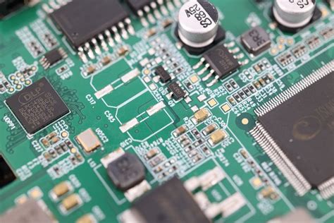
Reverse engineering multilayer printed circuit boards (PCBs) is a complex process that requires a combination of specialized tools and techniques. This intricate task involves deconstructing a PCB to understand its design and functionality, often for purposes such as troubleshooting, redesign, or competitive analysis. To begin with, one must have a clear understanding of the PCB’s structure, which typically consists of multiple layers of conductive and insulating materials. These layers are intricately connected through vias and traces, making the reverse engineering process particularly challenging.
The first step in reverse engineering a multilayer PCB is to gather the necessary tools.
Essential equipment includes a high-resolution scanner or a camera with macro capabilities to capture detailed images of the PCB. Additionally, a multimeter and an LCR meter are crucial for measuring electrical properties such as resistance, capacitance, and inductance. For more advanced analysis, an oscilloscope can be used to observe the electrical signals on the board. Furthermore, a desoldering station is indispensable for removing components without damaging the board, allowing for a closer inspection of the underlying traces and vias.
Once the tools are assembled, the process begins with a thorough visual inspection of the PCB.
This involves examining both sides of the board to identify components, traces, and any visible connections. It is beneficial to take high-resolution images of the board at this stage, as these images will serve as a reference throughout the reverse engineering process. Following the visual inspection, the next step is to carefully remove the components from the PCB using the desoldering station. This allows for a clearer view of the traces and vias, which are often obscured by the components.
With the components removed, the focus shifts to mapping the PCB’s layout.
This involves tracing the connections between different components and layers. Here, the high-resolution images taken earlier prove invaluable, as they can be used to digitally reconstruct the board’s layout using software tools. Programs such as Eagle, KiCad, or Altium Designer can assist in creating a schematic representation of the PCB. These tools allow for the overlaying of images and the manual tracing of connections, which is essential for understanding the board’s design.
In addition to mapping the layout, it is crucial to analyze the electrical characteristics of the PCB.
This is where the multimeter, LCR meter, and oscilloscope come into play. By measuring the resistance, capacitance, and inductance of various traces and components, one can gain insights into the board’s functionality. This data is vital for creating an accurate schematic and for understanding how the PCB operates under different conditions.
Throughout the reverse engineering process, documentation is key.
Keeping detailed notes on the connections, measurements, and observations made during each step will facilitate a comprehensive understanding of the PCB. This documentation will also be invaluable if the board needs to be reconstructed or if similar reverse engineering tasks are undertaken in the future.
In conclusion, reverse engineering a multilayer PCB is a meticulous process that requires a combination of specialized tools and techniques. By systematically inspecting, documenting, and analyzing the board, one can unravel its complexities and gain a deeper understanding of its design and functionality. This knowledge can then be applied to various applications, from troubleshooting and redesign to innovation and competitive analysis.

Step-By-Step Guide To Analyzing PCB Layers
Reverse engineering a multilayer printed circuit board (PCB) is a complex yet fascinating process that requires a meticulous approach to understand the intricate design and functionality of the board. This process is often undertaken to analyze the design for educational purposes, to troubleshoot issues, or to replicate a design for which documentation is unavailable. To begin with, it is essential to have a clear understanding of the tools and techniques required for this task. The primary tools include a high-resolution scanner or camera, a multimeter, and software for PCB design and analysis. Additionally, having a basic understanding of electronics and PCB design principles is crucial.
The first step in analyzing PCB layers is to carefully document the board’s physical characteristics.
This involves taking high-resolution images of both sides of the PCB. These images serve as a reference throughout the reverse engineering process. It is important to ensure that the images are clear and detailed, capturing all visible traces, components, and markings. Once the images are obtained, the next step is to identify and catalog all visible components. This includes noting the component values, types, and any identifiable markings or part numbers. This information is vital for understanding the board’s functionality and for sourcing replacement components if necessary.
Following the documentation of components, the next phase involves the removal of components from the PCB.
This step should be approached with caution to avoid damaging the board or the components. Using a soldering iron or a desoldering station, carefully desolder each component, taking care to note their original positions on the board. This step is crucial for gaining access to the underlying layers of the PCB. Once the components are removed, the board should be cleaned to remove any residual solder or flux, which can obscure traces and vias.
With the board cleaned and components removed, the focus shifts to analyzing the individual layers of the PCB.
Multilayer PCBs can have several layers, each serving a specific purpose, such as power distribution, signal routing, or ground planes. To analyze these layers, the board may need to be carefully sanded or chemically stripped to expose each layer. This process requires precision and patience, as excessive force can damage the delicate traces and vias. As each layer is exposed, it should be documented with high-resolution images, similar to the initial documentation process.
Once all layers are exposed and documented, the next step is to trace the connections and pathways on each layer.
This involves using the images to map out the electrical connections, noting how traces connect different components and layers. This step is often the most time-consuming, as it requires a detailed understanding of the board’s design and functionality. Software tools can assist in this process by allowing for the digital reconstruction of the PCB layout, making it easier to visualize and analyze the connections.
Finally, with a comprehensive understanding of the PCB’s design, the reverse engineering process concludes with the creation of a schematic diagram. This diagram serves as a blueprint of the board’s electrical design, detailing the connections and components. It is a valuable resource for troubleshooting, replication, or further analysis. Throughout this process, attention to detail and a methodical approach are paramount to successfully reverse engineering a multilayer PCB.
Common Challenges And Solutions In PCB Reverse Engineering
Reverse engineering a multilayer printed circuit board (PCB) is a complex process that involves several challenges, each requiring careful consideration and strategic solutions. One of the primary challenges in this endeavor is the intricate nature of multilayer PCBs themselves. These boards consist of multiple layers of conductive and insulating materials, which are laminated together to form a compact and efficient circuit. The complexity increases with the number of layers, making it difficult to access and analyze the internal structures without causing damage.
To address this challenge, one effective solution is the use of advanced imaging techniques.
X-ray imaging, for instance, allows engineers to visualize the internal layers of a PCB without physically dismantling it. This non-destructive method provides a clear view of the internal connections and components, enabling a more accurate analysis. Additionally, computed tomography (CT) scans can offer three-dimensional images, further enhancing the understanding of the board’s structure.
Another significant challenge in PCB reverse engineering is the identification and understanding of the components used.
Multilayer PCBs often incorporate a wide variety of components, each with specific functions and characteristics. Identifying these components requires a comprehensive knowledge of electronic components and their symbols. To overcome this, engineers can utilize component identification software, which can automatically recognize and catalog components based on their physical and electrical characteristics. This software can significantly reduce the time and effort required to manually identify each component.
Furthermore, the extraction of the schematic diagram from a multilayer PCB poses its own set of challenges.
The schematic is essential for understanding the circuit’s functionality and for replicating or modifying the design. However, due to the complexity of multilayer boards, tracing the connections between components can be daunting. To facilitate this process, engineers can employ specialized software tools that assist in generating schematic diagrams from PCB layouts. These tools can automatically trace connections and generate a preliminary schematic, which can then be refined and verified by the engineer.
In addition to these technical challenges, legal and ethical considerations also play a crucial role in PCB reverse engineering.
It is essential to ensure that the reverse engineering process complies with intellectual property laws and respects the original designer’s rights. Engineers must be aware of the legal implications and obtain necessary permissions or licenses before proceeding with reverse engineering activities. This not only protects the engineer from potential legal issues but also fosters a culture of respect and integrity within the industry.
Moreover, reverse engineering a multilayer PCB often requires a multidisciplinary approach, involving expertise in electronics, materials science, and software engineering.
Collaboration among professionals from these fields can lead to more effective solutions and innovative approaches to overcoming the challenges associated with PCB reverse engineering. By leveraging the diverse skills and knowledge of a multidisciplinary team, engineers can enhance their problem-solving capabilities and achieve more accurate and efficient results.
In conclusion, while reverse engineering multilayer PCBs presents numerous challenges, there are several solutions available to address these issues effectively. By utilizing advanced imaging techniques, component identification software, and schematic generation tools, engineers can navigate the complexities of multilayer PCBs with greater ease. Additionally, adhering to legal and ethical standards and fostering collaboration among multidisciplinary teams can further enhance the success of reverse engineering projects. Through these strategies, engineers can unlock the potential of existing PCB designs and contribute to the advancement of electronic technology.