Understanding BGA PCB Assembly Techniques and Benefits
Key Takeaways
BGA PCB assembly stands out as a critical process in modern electronics manufacturing, thanks to its ability to facilitate high-density designs and improve overall component performance. The BGA (Ball Grid Array) technology offers significant advantages over traditional packaging methods, primarily through its enhanced electrical performance and thermal management capabilities. As the demand for smaller and more efficient devices increases, companies are increasingly turning to BGA pcba solutions. One of the key benefits of this technology is its ability to reduce the required footprint on PCB layouts, allowing for more compact designs without sacrificing reliability. Furthermore, the soldering mechanism used in BGA assemblies ensures better mechanical strength and electrical connections than other methods. However, successful pcb assembly using BGA does come with challenges, such as precise alignment and solder joint quality control. By embracing established best practices, manufacturers can effectively address these challenges and optimize their production processes. Ultimately, understanding these foundational aspects of BGA PCB assembly will enable businesses to harness the full potential of this innovative technology in their electronic solutions.
Introduction to BGA PCB Assembly
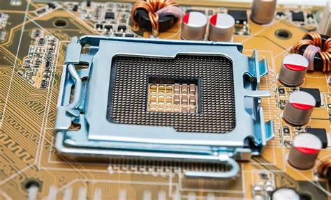
Ball Grid Array (BGA) technology has revolutionized the field of PCB assembly by providing a compact and efficient way to connect integrated circuits. This method involves arranging solder balls in a grid pattern on the bottom of a chip, offering a notable advantage in minimizing space on the circuit board. The shift towards BGAs from traditional surface mount technology underscores the necessity for enhanced performance in PCB assembly processes.
One of the most appealing facets of BGA PCB assembly is its ability to support higher pin counts without increasing board size, thereby facilitating improved functionality in electronic devices. The thermal and electrical performance associated with BGAs is remarkable, significantly reducing issues related to heat dissipation and enhancing signal integrity.
“Embracing advanced assembly techniques is crucial for staying competitive in the fast-evolving electronics landscape.”
Despite its advantages, implementing effective PCB assembly strategies requires an understanding of complex techniques such as precise placement and soldering. Ensuring reliability throughout the life cycle of an electronic product involves recognizing the unique challenges that come with BGAs, including potential voids during soldering and ensuring robust electrical connections. In navigating these intricacies, manufacturers can harness the full potential of BGA technology, making it an indispensable component in modern electronics manufacturing processes.
By exploring these aspects further, stakeholders can make informed decisions that drive efficiency and reliability within their operations while meeting market demands for increasingly sophisticated electronic devices.
Key Techniques in BGA PCB Assembly
BGA PCB assembly involves several intricate techniques that ensure reliability and performance in modern electronics. One of the primary methods utilized is reflow soldering, where solder paste is applied to the PCB pads, and then components are placed before they undergo a heating process. This technique is crucial because it allows for a strong bond between the BGA balls and the PCB, enhancing the overall electrical performance.
Another vital technique is X-ray inspection, which plays a significant role in verifying the integrity of the solder joints. This non-destructive method helps in identifying issues such as voids or insufficient solder, ensuring high-quality standards are maintained throughout the pcb assembly process.
Furthermore, the use of automated equipment for placement and inspection reduces human error, improving operational efficiency. In addition to these methods, employing a controlled environment during assembly can prevent issues related to contamination or humidity, thereby safeguarding both the components and final product quality.
Here’s a comparison table that highlights these key techniques:
| Technique | Description | Benefits |
|---|---|---|
| Reflow Soldering | Heating process to bond solder paste with components | Strong electrical connections |
| X-ray Inspection | Non-destructive testing for joint integrity | Early detection of defects |
| Automated Equipment | Machinery for placement and inspection | Reduced errors, increased efficiency |
| Controlled Environment | Maintained conditions during assembly | Minimizes contamination risks |
By integrating these essential techniques into the pcba workflow, manufacturers can greatly enhance both efficiency and reliability, ensuring that electronic devices perform optimally in their intended applications.
Advantages of BGA Technology in Electronics
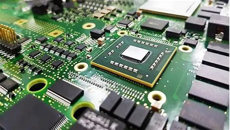
The use of BGA (Ball Grid Array) technology in pcb assembly has revolutionized modern electronics manufacturing, offering numerous advantages that enhance the performance and reliability of electronic devices. One notable benefit is the increased density of components that can be packed onto a board, which is particularly advantageous for compact designs in mobile devices and other consumer electronics. This increased density does not come at the expense of electrical performance; a well-executed pcba with BGA technology ensures superior thermal performance, helping to manage heat dissipation more effectively than older technologies.
Another significant advantage is the improved mechanical strength and stability of connections; unlike traditional pin-based packages, BGAs provide a larger surface area for soldering to the PCB, which reduces the likelihood of solder joint failure during thermal cycling or mechanical stress. Additionally, the inherent design minimizes problems related to electromagnetic interference, contributing to better overall functionality. BGA technology also supports advanced testing methods, allowing for in-circuit or functional testing without requiring disassembly. Overall, these advantages position BGA technology as a pivotal element in the future of pcb assembly, enabling manufacturers to meet increasingly demanding performance specifications while optimizing space and efficiency in their products.
Common Challenges and Solutions in BGA Assembly
BGA PCB assembly, while offering numerous advantages, presents several unique challenges that manufacturers must navigate. One prominent issue is void formation during soldering, which can lead to unreliable connections and affect the overall performance of the PCB assembly. To address this, manufacturers often employ techniques such as optimal heat profiles and the use of specialized solder paste formulations designed to minimize voids. Additionally, the pcba process can be complicated by misalignment of components, which may arise during assembly or reflow stages. Utilizing advanced alignment technologies and automated inspection systems can significantly mitigate this risk. Another common challenge is the thermal management of high-density BGA packages; inadequate thermal management can lead to overheating and performance degradation. Implementing proper thermal via designs and careful placement of heat sinks can enhance thermal performance. Furthermore, managing solder joint reliability over time remains a concern due to potential mechanical stresses on BGAs. By conducting thorough mechanical analysis and adopting flexible mounting techniques, these stresses can be effectively reduced. Overall, addressing these challenges through a combination of innovative solutions and best practices ensures that BGA technology remains a reliable choice in modern electronics manufacturing.
Best Practices for Efficient BGA PCB Manufacturing
When it comes to BGA PCB assembly, adopting best practices is crucial for enhancing both efficiency and reliability in the manufacturing process. First and foremost, utilizing high-quality materials is imperative. This includes opting for reliable solder paste and well-designed PCB substrates that ensure optimal connection integrity. Additionally, implementing a robust printing technique is essential; precise stencil alignment and paste application can significantly reduce solder defects. It’s also beneficial to maintain strict temperature control during the reflow process to prevent thermal shock which can damage components.
Moreover, thorough testing protocols such as automated optical inspection (AOI) and X-ray inspection should be routinely utilized. These methods help identify defects early on, saving time and reducing costs associated with post-assembly repairs. Another practice involves rigorous documentation of the pcba processes; maintaining records of material specifications, assembly steps, and test results promotes a culture of consistency and quality assurance.
Lastly, fostering ongoing training for personnel involved in the BGA assembly process can also yield great benefits. Educating workers about the intricacies of BGA technology, including issues surrounding component placement and soldering techniques, enhances overall operational efficiency. Ultimately, by implementing these best practices in BGA PCB assembly, manufacturers can achieve a significant improvement in both productivity and product integrity in modern electronics manufacturing.
Quality Control Measures for BGA Assemblies
Ensuring the highest standards of quality in BGA PCB assembly is crucial for the reliability and performance of electronic devices. One of the primary quality control measures involves rigorous inspection techniques, such as Automated Optical Inspection (AOI), which plays a pivotal role in detecting defects early in the pcba process. This technology helps identify issues like misaligned components or solder defects that might compromise the functionality of the assembly. Moreover, employing X-ray inspection can further enhance quality assurance by allowing manufacturers to examine hidden solder joints that are not visible through standard inspection methods.
Additionally, proper thermal profiling is essential during the reflow process to ensure that all joints receive adequate heat while minimizing thermal stress. Consistency in this phase helps prevent common problems such as cold solder joints, which can lead to failures in pcb assemblies under operational conditions. Integrating statistical process control (SPC) into manufacturing processes is another effective strategy that allows continuous monitoring and adjustment of parameters, thereby refining overall production quality.
Furthermore, establishing stringent environmental control measures during both assembly and testing phases contributes significantly to preventing contamination and ensuring optimal performance of components within BGA PCB assemblies. Regular audits and adherence to well-defined best practices, including adherence to industry standards such as IPC-610, bolster confidence in product reliability while maintaining compliance with customer demands for high-quality electronic manufacturing solutions.
Future Trends in BGA PCB Technologies
As the electronics industry continues to evolve, BGA PCB assembly techniques are poised for significant advancements. One of the primary trends is the integration of more sophisticated automated systems that enhance the speed and precision of pcba processes. Automation not only reduces human error but also increases production efficiency, thereby enabling manufacturers to meet the growing consumer demand for smaller yet more powerful devices. Additionally, the advent of advanced materials, including flexible substrates and innovative soldering technologies, is transforming how BGA assemblies are designed and produced. These materials offer improved thermal management and reliability, which are crucial for high-performance electronics. Another trend gaining traction is the adoption of artificial intelligence in quality control measures, allowing for real-time monitoring and defect detection during pcb assembly. This proactive approach helps to ensure product quality and minimizes waste, further contributing to overall efficiency. The trend toward miniaturization in gadgets also drives innovations in BGA technology, as manufacturers strive to create compact solutions without compromising functionality. By keeping abreast of these trends, companies can leverage new opportunities within pcba, ultimately leading to enhanced performance and reliability in modern electronics manufacturing.
Conclusion
In summary, BGA PCB assembly is a pivotal technique in the realm of modern electronics manufacturing, offering significant advantages in terms of efficiency and reliability. The intricate nature of this process demands a keen understanding of both the techniques involved and the specific benefits afforded by using BGA technology. Manufacturers who prioritize effective pcba practices can navigate common challenges by implementing rigorous quality control measures, which ultimately enhances overall production outcomes. As industries continue to evolve, the emphasis on advanced pcb assembly methods such as BGA will likely increase, paving the way for innovative solutions and improvements in electronic device performance. Embracing these methodologies not only optimizes current practices but also positions manufacturers at the forefront of technological advancements in the ever-competitive landscape of electronics.
FAQs
What is BGA PCB assembly?
BGA PCB assembly, or Ball Grid Array PCB Assembly, involves soldering electronic components that have solder balls on the underside, arranged in a grid pattern. This method enhances connectivity and facilitates high-density component placement on the PCB.
What are the benefits of using BGA technology?
The benefits of BGA technology include improved thermal performance, better electrical conductivity, and reduced inductance. Additionally, they support higher pin counts in a smaller footprint, making them ideal for modern electronics manufacturing.
What challenges are associated with BGA PCB assembly?
Common challenges include alignment issues during placement, difficulties in inspection due to hidden solder joints, and potential thermal stress on sensitive components. These challenges can be addressed through meticulous process control and advanced inspection techniques.
How can one ensure quality during BGA assembly?
Quality control measures such as automated optical inspection (AOI), X-ray inspection for solder joints, and strict adherence to manufacturing guidelines are essential for ensuring high-quality pcb assembly.