How pcb manufacturing process
Understanding The Basics Of PCB Manufacturing
Printed Circuit Boards (PCBs) are the backbone of modern electronic devices, serving as the foundation upon which electronic components are mounted and interconnected. Understanding the basics of PCB manufacturing is essential for anyone involved in electronics design and production.
The process begins with the design phase, where engineers use specialized software to create a schematic diagram and layout of the circuit.
This design is then translated into a digital file, typically in the form of Gerber files, which serve as the blueprint for the PCB.
Once the design is finalized, the manufacturing process commences with the selection of the base material, usually a fiberglass-reinforced epoxy laminate known as FR-4.
This material provides the necessary structural support and insulation for the conductive pathways. The next step involves the application of a thin layer of copper to both sides of the board, which will form the conductive traces. This is achieved through a process called lamination, where heat and pressure are applied to bond the copper to the substrate.
Following lamination, the board undergoes a process known as photoresist application.
A light-sensitive film is applied to the copper surface, and the board is exposed to ultraviolet light through a photomask that corresponds to the circuit design. The areas exposed to light harden, while the unexposed areas remain soft and are subsequently removed, revealing the copper traces that form the circuit pattern.
The next stage is etching, where a chemical solution is used to remove the unwanted copper, leaving only the desired circuit pattern intact.
This is a critical step, as precision is paramount to ensure the functionality of the final product. After etching, the board is cleaned to remove any residual chemicals and debris.
Drilling is the subsequent phase, where holes are created for component leads and vias, which are conductive pathways that connect different layers of the PCB.
Advanced drilling machines equipped with computer numerical control (CNC) technology ensure accuracy and consistency in hole placement and size.
Once drilling is complete, the board undergoes a plating process to deposit a thin layer of metal, typically copper, into the drilled holes. This step is crucial for establishing electrical connections between the different layers of the PCB. The board is then coated with a solder mask, a protective layer that insulates the copper traces and prevents solder bridges during component assembly. The solder mask is usually green, although other colors are available.
The final step in the PCB manufacturing process is the application of a silkscreen layer, which provides labels and markings for component placement and identification.
This layer is printed onto the board using a specialized ink that withstands the soldering process.
In conclusion, the PCB manufacturing process is a complex and precise series of steps that transform a digital design into a physical circuit board. Each stage, from design to final inspection, requires meticulous attention to detail to ensure the reliability and performance of the finished product. Understanding these basics provides valuable insight into the intricate world of electronics manufacturing, highlighting the importance of precision and quality control in producing the essential components that power our modern technological landscape.
Key Steps In The PCB Fabrication Process
The process of manufacturing printed circuit boards (PCBs) is a complex and intricate procedure that involves several key steps, each crucial to ensuring the final product meets the required specifications and quality standards. Understanding these steps provides insight into how electronic devices are brought to life, as PCBs serve as the backbone of most electronic systems.
Initially, the process begins with the design phase, where engineers use specialized software to create a detailed blueprint of the PCB .
This design outlines the layout of the circuit, including the placement of components and the routing of electrical connections. Once the design is finalized, it is converted into a format suitable for manufacturing, typically a Gerber file, which serves as a digital representation of the PCB layout.
Following the design phase, the next step is the preparation of the substrate, which forms the base of the PCB.
The substrate is usually made from a non-conductive material such as fiberglass, which provides structural support. A thin layer of copper is then laminated onto the substrate, as copper is an excellent conductor of electricity. This copper layer will eventually form the circuit paths that connect various components on the board.
The subsequent step involves transferring the circuit design onto the copper-clad substrate.
This is achieved through a process known as photolithography. During photolithography, a photosensitive film is applied to the copper surface, and the design is projected onto this film using ultraviolet light. The areas exposed to the light harden, while the unexposed areas remain soft and are subsequently washed away, leaving behind a precise pattern of the circuit design on the copper.
Once the circuit pattern is established, the next step is etching, where the excess copper is removed, leaving only the desired circuit paths.
This is typically done using a chemical solution that dissolves the unwanted copper. After etching, the board undergoes a thorough cleaning process to remove any residual chemicals and ensure the integrity of the circuit paths.
Following etching, the PCB is drilled to create holes for component leads and vias, which are used to connect different layers of the board.
Precision drilling is essential, as any misalignment can lead to connectivity issues. Once drilled, the holes are plated with copper to establish electrical connections between layers.
The next phase involves applying a solder mask, which is a protective layer that covers the circuit paths, leaving only the areas where components will be soldered exposed.
This mask prevents accidental short circuits and protects the copper from environmental damage. Additionally, a silkscreen layer is applied to the board, providing labels and markings that assist in component placement and identification.
Finally, the PCB undergoes a series of inspections and tests to ensure it meets all design and quality standards.
These tests may include electrical testing to verify connectivity and functionality, as well as visual inspections to check for any physical defects. Once the board passes these tests, it is ready for assembly, where electronic components are soldered onto the board, completing the manufacturing process.
In conclusion, the PCB fabrication process is a meticulous and multi-step procedure that transforms a digital design into a physical product. Each step, from design to testing, plays a vital role in ensuring the reliability and performance of the final PCB, which is essential for the functionality of electronic devices.

Innovations In PCB Manufacturing Technology
The field of printed circuit board (PCB) manufacturing has witnessed significant innovations over the years, driven by the relentless pursuit of efficiency, precision, and miniaturization. As electronic devices become increasingly complex and compact, the demand for advanced PCB manufacturing technologies has surged.
One of the most notable innovations in this domain is the advent of automated optical inspection (AOI) systems.
These systems have revolutionized the quality control process by enabling rapid and accurate detection of defects in PCBs. By utilizing high-resolution cameras and sophisticated algorithms, AOI systems can identify issues such as misalignments, soldering defects, and surface irregularities with remarkable precision. This not only enhances the reliability of the final product but also reduces the time and cost associated with manual inspections.
In addition to AOI, the integration of laser direct imaging (LDI) technology has marked a significant leap forward in PCB manufacturing.
LDI allows for the direct transfer of circuit patterns onto the PCB substrate using laser beams, eliminating the need for traditional photomasks. This innovation not only improves the accuracy of the patterning process but also facilitates rapid prototyping and customization. As a result, manufacturers can respond more swiftly to design changes and produce small batches of PCBs with minimal lead time. Furthermore, LDI technology contributes to the reduction of material waste, aligning with the growing emphasis on sustainable manufacturing practices.
Another transformative development in PCB manufacturing is the use of advanced materials, such as high-frequency laminates and flexible substrates.
These materials cater to the evolving needs of modern electronics, which often require PCBs to operate at higher frequencies and fit into unconventional form factors. High-frequency laminates, for instance, are engineered to minimize signal loss and electromagnetic interference, making them ideal for applications in telecommunications and aerospace. Meanwhile, flexible substrates enable the creation of bendable and foldable PCBs, opening up new possibilities for wearable technology and compact electronic devices.
Moreover, the implementation of Industry 4.0 principles has further propelled innovations in PCB manufacturing.
By leveraging the Internet of Things (IoT), big data analytics, and artificial intelligence (AI), manufacturers can optimize production processes and enhance decision-making. IoT-enabled sensors can monitor equipment performance in real-time, allowing for predictive maintenance and minimizing downtime. Big data analytics, on the other hand, provides valuable insights into production trends and customer preferences, enabling manufacturers to fine-tune their operations and product offerings. AI-driven algorithms can also assist in the design phase, suggesting optimal layouts and configurations based on vast datasets of previous designs.
Furthermore, the rise of additive manufacturing, commonly known as 3D printing, has introduced new dimensions to PCB fabrication.
While traditional subtractive methods involve etching away unwanted material, additive manufacturing builds PCBs layer by layer, offering greater design flexibility and material efficiency. This approach is particularly advantageous for producing complex, multi-layered PCBs with intricate geometries. As 3D printing technology continues to evolve, it holds the potential to further streamline the PCB manufacturing process and reduce production costs.
In conclusion, the landscape of PCB manufacturing is continually evolving, driven by technological advancements and the ever-increasing demands of the electronics industry. Innovations such as automated optical inspection, laser direct imaging, advanced materials, Industry 4.0 integration, and additive manufacturing are reshaping the way PCBs are designed and produced. These developments not only enhance the quality and performance of PCBs but also contribute to more sustainable and efficient manufacturing practices. As the industry progresses, it is likely that further breakthroughs will continue to emerge, paving the way for even more sophisticated electronic devices.
Quality Control Measures In PCB Production
In the intricate world of printed circuit board (PCB) manufacturing, quality control measures are paramount to ensure the reliability and functionality of the final product. The process of PCB production involves multiple stages, each requiring meticulous attention to detail to prevent defects and ensure that the boards meet stringent industry standards. As the demand for high-performance electronic devices continues to grow, the importance of robust quality control measures in PCB production cannot be overstated.
To begin with, the initial stage of PCB manufacturing involves the design and layout of the circuit.
This phase is crucial as it sets the foundation for the entire production process. Advanced software tools are employed to create precise designs, which are then rigorously reviewed to identify potential errors. This pre-production scrutiny helps in minimizing design flaws that could lead to functional failures in the final product. Once the design is finalized, it is converted into a photomask, which is used in the subsequent etching process.
Transitioning to the fabrication stage, the quality control measures become even more critical.
During etching, unwanted copper is removed from the board to create the desired circuit patterns. This process must be carefully monitored to ensure that the etching is uniform and that no excess material remains. Any deviation can result in short circuits or open circuits, compromising the board’s performance. To prevent such issues, manufacturers employ automated optical inspection (AOI) systems that use high-resolution cameras to detect defects at this early stage.
As the production progresses to the drilling and plating stages, precision remains a key focus.
Drilling involves creating holes for component leads and vias, which are essential for electrical connectivity. The accuracy of these holes is vital, as any misalignment can affect the board’s functionality. Quality control measures at this stage include the use of computer-controlled drilling machines and regular inspections to ensure that the holes are correctly positioned and of the appropriate size.
Following drilling, the boards undergo a plating process to deposit a thin layer of metal, typically copper, onto the drilled holes.
This step is crucial for establishing electrical connections between different layers of the PCB. Quality control during plating involves monitoring the thickness and uniformity of the metal layer, as inconsistencies can lead to poor conductivity and potential failures in the field.
As the PCB nears completion, solder mask application and silkscreen printing are performed.
The solder mask is a protective layer that prevents solder bridges between closely spaced components, while the silkscreen provides labels and markings for component placement. Quality control measures here include visual inspections and AOI to ensure that the solder mask is accurately applied and that the silkscreen is legible and correctly aligned.
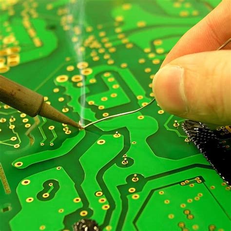
Finally, the assembled PCBs undergo functional testing to verify their performance.
This involves subjecting the boards to various electrical tests to ensure that they operate as intended. Any defects identified during testing are addressed before the boards are approved for shipment. This final quality control step is crucial in guaranteeing that the PCBs meet the required specifications and are free from defects that could affect their performance in real-world applications.
In conclusion, quality control measures in PCB production are integral to ensuring the reliability and functionality of the final product. From design verification to functional testing, each stage of the manufacturing process incorporates rigorous checks to prevent defects and ensure compliance with industry standards. As technology continues to advance, the emphasis on quality control in PCB production will remain a critical factor in delivering high-performance electronic devices.