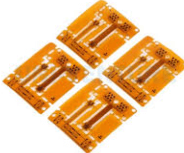
High speed pcb practice layouts
Optimizing Signal Integrity in High-Speed PCB Layouts
In the realm of modern electronics, the demand for high-speed printed circuit boards (PCBs) has surged, driven by the need for faster data processing and communication. As devices become more sophisticated, ensuring signal integrity in high-speed PCB layouts has become a critical aspect of design. Signal integrity refers to the preservation of the quality of electrical signals as they travel through the PCB, and optimizing it is essential to prevent data loss and ensure reliable device performance.
To begin with, understanding the fundamental principles of signal integrity is crucial.
High-speed signals are susceptible to various forms of interference, such as crosstalk, reflection, and electromagnetic interference (EMI). These issues can distort signals, leading to errors and reduced performance. Therefore, designers must employ strategies to mitigate these effects. One effective approach is to carefully consider the trace layout. Traces should be kept as short as possible to minimize inductance and resistance, which can degrade signal quality. Additionally, maintaining consistent trace widths and spacing helps to reduce impedance discontinuities, which can cause reflections.
Moreover, the use of ground planes is a vital practice in high-speed PCB design.
Ground planes provide a return path for signals, reducing loop inductance and minimizing EMI. By placing a continuous ground plane beneath signal traces, designers can create a controlled impedance environment, which is essential for maintaining signal integrity. Furthermore, ground planes help to shield sensitive traces from external noise sources, further enhancing signal quality.
Transitioning to the topic of layer stack-up, it is important to note that the arrangement of layers in a PCB can significantly impact signal integrity.
A well-planned layer stack-up can help control impedance and reduce crosstalk. Typically, high-speed PCBs employ a multi-layer stack-up, with dedicated layers for power, ground, and signal routing. This configuration allows for better separation of signals and reduces the potential for interference. Additionally, using differential pairs for high-speed signals can further enhance signal integrity. Differential pairs consist of two traces carrying equal and opposite signals, which helps to cancel out noise and improve signal quality.
Another critical aspect of optimizing signal integrity is the careful selection of materials.
The dielectric material used in the PCB can affect signal propagation speed and loss. Low-loss materials are preferred for high-speed applications, as they minimize signal attenuation and ensure faster signal transmission. Additionally, the choice of solder mask and surface finish can influence signal integrity. For instance, using a thin solder mask can reduce parasitic capacitance, while selecting an appropriate surface finish can improve signal quality by reducing signal loss at high frequencies.
In conclusion, optimizing signal integrity in high-speed PCB layouts is a multifaceted challenge that requires careful consideration of various design elements.
By focusing on trace layout, ground planes, layer stack-up, and material selection, designers can significantly enhance signal quality and ensure reliable device performance. As technology continues to advance, the importance of maintaining signal integrity in high-speed PCBs will only grow, making it an essential area of focus for engineers and designers alike. Through meticulous design practices and a thorough understanding of signal integrity principles, the challenges posed by high-speed PCB layouts can be effectively addressed, paving the way for the next generation of high-performance electronic devices.
Best Practices for Layer Stackup in High-Speed PCB Design
In the realm of high-speed printed circuit board (PCB) design, the layer stackup plays a pivotal role in ensuring optimal performance and reliability. As electronic devices become increasingly complex, the demand for high-speed data transmission has surged, necessitating meticulous attention to the intricacies of PCB design. A well-considered layer stackup not only enhances signal integrity but also mitigates electromagnetic interference (EMI), which is crucial for maintaining the functionality of high-speed circuits.
To begin with, understanding the fundamental principles of layer stackup is essential.
A typical high-speed PCB consists of multiple layers, each serving a specific purpose. The arrangement of these layers can significantly impact the electrical performance of the board. For instance, signal layers, which carry the high-speed signals, should be strategically placed to minimize crosstalk and signal loss. By positioning these layers adjacent to ground or power planes, designers can create a controlled impedance environment, which is vital for maintaining signal integrity.
Moreover, the choice of materials for each layer is another critical consideration.
High-speed PCBs often require materials with low dielectric constants and low loss tangents to reduce signal attenuation. These materials help in preserving the signal quality over long distances, which is particularly important in high-frequency applications. Additionally, selecting materials with consistent dielectric properties across the board can prevent signal distortion, thereby enhancing the overall performance of the PCB.
Transitioning to the topic of power distribution, it is imperative to design a robust power delivery network (PDN) within the layer stackup.
A well-designed PDN ensures that power is distributed evenly across the board, minimizing voltage drops and power supply noise. This can be achieved by incorporating dedicated power and ground planes, which provide low-impedance paths for current flow. Furthermore, placing decoupling capacitors close to power pins can help in stabilizing the power supply, reducing the risk of signal degradation.
Another aspect to consider is the thermal management of high-speed PCBs.
As data rates increase, so does the power consumption, leading to potential thermal issues. Effective thermal management can be achieved by optimizing the layer stackup to facilitate heat dissipation. For example, using thicker copper layers can enhance thermal conductivity, while strategically placing thermal vias can help in transferring heat away from critical components. This not only prolongs the lifespan of the PCB but also ensures reliable operation under high-speed conditions.
In addition to these technical considerations, adhering to industry standards and guidelines is crucial for successful high-speed PCB design.
Standards such as IPC-2221 and IPC-2222 provide comprehensive guidelines on layer stackup configurations, material selection, and design practices. By following these standards, designers can ensure that their PCBs meet the necessary performance and reliability criteria.
In conclusion, the layer stackup is a fundamental aspect of high-speed PCB design that requires careful planning and execution. By understanding the principles of layer arrangement, material selection, power distribution, and thermal management, designers can create PCBs that not only meet the demands of high-speed applications but also exhibit superior performance and reliability. As technology continues to evolve, staying abreast of the latest advancements and best practices in layer stackup design will be essential for engineers striving to push the boundaries of high-speed electronics.

Managing Crosstalk and EMI in High-Speed PCB Layouts
In the realm of high-speed printed circuit board (PCB) design, managing crosstalk and electromagnetic interference (EMI) is paramount to ensuring optimal performance and reliability. As electronic devices become increasingly complex and compact, the challenges associated with high-speed PCB layouts have intensified. Crosstalk, which refers to the unwanted coupling of signals between adjacent traces, and EMI, the disturbance generated by electromagnetic fields, can significantly degrade the performance of a PCB if not properly managed. Therefore, understanding and implementing effective strategies to mitigate these issues is crucial for engineers and designers.
To begin with, one of the fundamental strategies in managing crosstalk is maintaining adequate spacing between signal traces.
By increasing the distance between traces, the capacitive and inductive coupling that leads to crosstalk can be minimized. Additionally, employing differential signaling, where two complementary signals are routed together, can further reduce crosstalk. This technique not only helps in canceling out noise but also enhances signal integrity. Moreover, the use of ground planes is another effective method to combat crosstalk. Ground planes act as a shield, reducing the electromagnetic field coupling between traces and providing a return path for signals, thereby minimizing interference.
Transitioning to the topic of EMI, it is essential to consider the layout of components and traces on the PCB.
A well-thought-out layout can significantly reduce EMI emissions. For instance, placing high-speed components closer to the power source and minimizing the loop area of high-frequency signals can help in reducing EMI. Furthermore, the use of decoupling capacitors is a common practice to suppress high-frequency noise. These capacitors, placed close to the power pins of integrated circuits, help in stabilizing the power supply and reducing voltage fluctuations that can lead to EMI.
In addition to layout considerations, the choice of materials also plays a critical role in managing crosstalk and EMI.
High-speed PCBs often require materials with low dielectric constants and low loss tangents to ensure signal integrity. These materials help in reducing signal attenuation and maintaining the integrity of high-frequency signals. Moreover, the use of shielding techniques, such as enclosing sensitive components in metal enclosures or using shielded cables, can further mitigate EMI.
Another important aspect to consider is the implementation of proper grounding techniques.
A solid grounding strategy is essential for minimizing both crosstalk and EMI. Ensuring a low-impedance path to ground and avoiding ground loops can significantly reduce interference. Additionally, the use of vias to connect different layers of the PCB can help in maintaining a consistent ground reference, further enhancing the board’s performance.
In conclusion, managing crosstalk and EMI in high-speed PCB layouts requires a comprehensive approach that encompasses various design strategies and considerations. By maintaining adequate trace spacing, employing differential signaling, utilizing ground planes, optimizing component layout, selecting appropriate materials, and implementing effective grounding techniques, designers can significantly mitigate the adverse effects of crosstalk and EMI. As technology continues to advance, the importance of these practices will only grow, underscoring the need for designers to stay informed and adept in the latest high-speed PCB design methodologies.
Via Design Techniques for High-Speed PCB Performance
In the realm of high-speed printed circuit board (PCB) design, the meticulous arrangement of vias plays a pivotal role in ensuring optimal performance. As electronic devices continue to demand faster processing speeds and greater data throughput, the need for effective via design techniques becomes increasingly critical. Vias, which are the conductive pathways that connect different layers of a PCB, can significantly impact signal integrity, electromagnetic interference, and overall board performance. Therefore, understanding and implementing best practices in via design is essential for engineers striving to achieve high-speed PCB performance.
To begin with, it is important to recognize that vias introduce discontinuities in the signal path, which can lead to reflections and signal degradation.
This is particularly problematic in high-speed applications where even minor disruptions can result in significant performance issues. One effective technique to mitigate these effects is the use of via stubs. Via stubs are the unused portions of a via that extend beyond the signal layer. By minimizing or eliminating these stubs, designers can reduce the potential for signal reflections and improve signal integrity. Techniques such as back-drilling, where the unused portion of the via is drilled out, are commonly employed to address this issue.
Moreover, the placement and distribution of vias on a PCB can greatly influence its performance.
Clustering vias too closely can lead to crosstalk, where signals from one via interfere with those in adjacent vias. To prevent this, designers should ensure adequate spacing between vias, adhering to the design rules specific to the board’s operating frequency. Additionally, staggering vias rather than aligning them in a straight line can further reduce the risk of crosstalk and improve overall signal quality.
Another crucial aspect of via design is the consideration of via impedance.
Vias inherently possess inductance and capacitance, which can affect the impedance of the signal path. To maintain consistent impedance, it is advisable to use vias with a consistent diameter and to ensure that the via’s barrel is properly plated. Furthermore, employing techniques such as via-in-pad, where the via is placed directly within the pad of a component, can help minimize inductance and improve signal performance. However, this approach requires careful consideration of manufacturing capabilities and potential challenges in solderability.
Thermal management is another factor that must be taken into account when designing vias for high-speed PCBs.
Vias can serve as thermal conduits, dissipating heat away from critical components. By strategically placing thermal vias near heat-generating components, designers can enhance the thermal performance of the board. This is particularly important in high-speed applications where excessive heat can lead to component failure and reduced reliability.
In addition to these technical considerations, it is essential for designers to collaborate closely with manufacturers to ensure that the chosen via design techniques are compatible with the fabrication process. This collaboration can help identify potential manufacturing constraints and ensure that the final product meets the desired performance specifications.
In conclusion, via design techniques are a fundamental aspect of high-speed PCB performance. By carefully considering factors such as via stubs, placement, impedance, and thermal management, designers can significantly enhance the signal integrity and overall performance of their boards. As technology continues to advance, the importance of effective via design will only grow, making it a critical area of focus for engineers in the field of high-speed PCB design.