High speed pcb manufacturing
Innovations In High Speed PCB Manufacturing Techniques
In recent years, the demand for high-speed printed circuit boards (PCBs) has surged, driven by the rapid advancement of technology and the need for faster, more efficient electronic devices. As a result, innovations in high-speed PCB manufacturing techniques have become crucial to meet these demands. These innovations not only enhance the performance of electronic devices but also ensure reliability and cost-effectiveness in production.
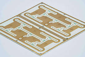
One of the most significant advancements in high-speed PCB manufacturing is the development of advanced materials.
Traditional materials, such as FR-4, are often inadequate for high-speed applications due to their limited electrical performance. Consequently, manufacturers have turned to high-frequency laminates, which offer superior dielectric properties and reduced signal loss. These materials are essential for maintaining signal integrity in high-speed applications, such as telecommunications and data centers, where even minor signal degradation can lead to significant performance issues.
In addition to material innovations, the design of high-speed PCBs has also evolved.
Modern design techniques focus on minimizing signal interference and crosstalk, which are critical factors in high-speed applications. Techniques such as controlled impedance routing and differential pair routing have become standard practices. These methods ensure that signals are transmitted with minimal distortion, thereby enhancing the overall performance of the PCB. Moreover, the use of simulation software has become indispensable in the design phase, allowing engineers to model and predict the behavior of high-speed signals before the physical board is manufactured.
Another key innovation in high-speed PCB manufacturing is the adoption of advanced fabrication processes.
Traditional etching and drilling methods are often insufficient for the precision required in high-speed applications. Therefore, manufacturers have embraced laser drilling and direct imaging technologies, which offer greater accuracy and finer feature sizes. These technologies enable the production of complex multilayer boards with high-density interconnects, which are essential for accommodating the increased number of components and connections in modern electronic devices.
Furthermore, the integration of automated manufacturing processes has revolutionized high-speed PCB production.
Automation not only increases production efficiency but also reduces the likelihood of human error, which can be detrimental in high-speed applications. Automated optical inspection (AOI) and automated X-ray inspection (AXI) systems are now commonly used to ensure the quality and reliability of PCBs. These systems provide real-time feedback and allow for immediate corrections, thereby minimizing defects and improving yield rates.
The role of thermal management in high-speed PCB manufacturing cannot be overlooked.
As electronic devices become more powerful, they generate more heat, which can adversely affect performance and reliability. Innovations in thermal management techniques, such as the use of thermal vias and heat sinks, have become essential. These methods help dissipate heat effectively, ensuring that the PCB operates within safe temperature limits.
In conclusion, the innovations in high-speed PCB manufacturing techniques have been instrumental in meeting the growing demands of modern electronic applications. From advanced materials and design techniques to precision fabrication processes and automated inspections, these innovations ensure that high-speed PCBs deliver optimal performance and reliability. As technology continues to evolve, it is likely that further advancements will emerge, driving the industry towards even greater heights of efficiency and capability.
Challenges And Solutions In High Speed PCB Design
High-speed PCB manufacturing is a critical component in the development of modern electronic devices, where the demand for faster processing speeds and higher data rates continues to grow. As technology advances, the challenges associated with designing and manufacturing high-speed printed circuit boards (PCBs) become increasingly complex. These challenges necessitate innovative solutions to ensure that the final product meets the required performance standards while maintaining reliability and cost-effectiveness.
One of the primary challenges in high-speed PCB design is signal integrity.
As data rates increase, the potential for signal degradation due to factors such as crosstalk, reflection, and electromagnetic interference (EMI) also rises. Crosstalk occurs when a signal transmitted on one trace interferes with a signal on an adjacent trace, leading to data corruption. To mitigate this, designers must carefully consider trace spacing and routing techniques. Additionally, the use of differential signaling, where two complementary signals are sent over a pair of traces, can help reduce the effects of crosstalk and improve signal integrity.
Reflection is another significant issue that arises from impedance mismatches along the transmission path.
When the impedance of the trace does not match the source or load, part of the signal is reflected back towards the source, causing distortion. To address this, designers must ensure that the characteristic impedance of the traces is consistent throughout the PCB. This can be achieved through controlled impedance design, which involves selecting appropriate materials and trace geometries to maintain uniform impedance.
Electromagnetic interference is a pervasive challenge in high-speed PCB design, as it can lead to unwanted noise and signal distortion.
Shielding techniques, such as the use of ground planes and proper grounding strategies, are essential in minimizing EMI. Moreover, incorporating decoupling capacitors near power pins can help filter out high-frequency noise, further enhancing signal integrity.
Thermal management is another critical aspect of high-speed PCB design.
As components operate at higher speeds, they generate more heat, which can adversely affect performance and reliability. Effective thermal management strategies, such as the use of thermal vias, heat sinks, and appropriate material selection, are crucial in dissipating heat and maintaining optimal operating temperatures.
In addition to these technical challenges, high-speed PCB manufacturing also faces logistical and economic hurdles.
The complexity of high-speed designs often results in increased production costs and longer lead times. To address these issues, manufacturers are turning to advanced fabrication techniques, such as laser drilling and precision etching, which allow for greater accuracy and efficiency in the production process. Furthermore, the adoption of automated design tools and simulation software enables designers to optimize their layouts and identify potential issues early in the design phase, reducing the likelihood of costly revisions.
In conclusion, the challenges associated with high-speed PCB design are multifaceted, encompassing signal integrity, thermal management, and manufacturing complexities. However, through the implementation of innovative solutions and advanced technologies, these challenges can be effectively addressed. As the demand for high-speed electronic devices continues to rise, the ability to overcome these obstacles will be crucial in ensuring the successful development and deployment of next-generation technologies. By staying at the forefront of design and manufacturing advancements, the industry can continue to meet the evolving needs of consumers and maintain its competitive edge in the global market.
The Role Of Material Selection In High Speed PCB Performance
In the realm of high-speed printed circuit board (PCB) manufacturing, the selection of materials plays a pivotal role in determining the overall performance and reliability of the final product. As electronic devices continue to evolve, demanding faster processing speeds and greater data transmission capabilities, the need for high-speed PCBs has become increasingly critical. Consequently, understanding the impact of material selection on high-speed PCB performance is essential for engineers and manufacturers striving to meet these technological demands.
To begin with, the dielectric material used in a PCB is a fundamental factor influencing its high-speed performance.
Dielectric materials are responsible for insulating the conductive layers within the PCB, and their properties significantly affect signal integrity. A key parameter to consider is the dielectric constant (Dk), which measures a material’s ability to store electrical energy. Materials with a lower Dk are generally preferred for high-speed applications because they reduce signal delay and minimize signal distortion. Additionally, the dissipation factor (Df), which quantifies the energy loss as heat, should be low to ensure efficient signal transmission. Therefore, selecting materials with optimal Dk and Df values is crucial for maintaining signal integrity in high-speed PCBs.
Moreover, the thermal properties of the materials used in high-speed PCBs cannot be overlooked.
As electronic components operate at higher speeds, they generate more heat, which can adversely affect performance and reliability. Materials with high thermal conductivity are essential to dissipate heat effectively, preventing overheating and ensuring the longevity of the PCB. Furthermore, the coefficient of thermal expansion (CTE) is another critical consideration. A mismatch in CTE between the PCB material and the components can lead to mechanical stress and potential failure. Thus, selecting materials with compatible CTE values is vital for maintaining structural integrity under thermal cycling conditions.
In addition to dielectric and thermal properties, the mechanical characteristics of PCB materials also play a significant role in high-speed applications.
The material’s rigidity and flexibility can impact the board’s ability to withstand mechanical stresses during manufacturing and operation. For instance, materials with high tensile strength and flexibility are advantageous in applications where the PCB may be subject to bending or vibration. This ensures that the board maintains its structural integrity and continues to function optimally in demanding environments.
Furthermore, the choice of conductive materials, such as copper, is equally important in high-speed PCB manufacturing.
The thickness and quality of the copper layers influence the board’s electrical performance, including its ability to handle high-frequency signals. Thinner copper layers can reduce signal loss and improve impedance control, which is crucial for maintaining signal integrity at high speeds. Additionally, surface finishes applied to the copper, such as immersion gold or silver, can enhance conductivity and protect against oxidation, further contributing to the board’s performance.
In conclusion, the role of material selection in high-speed PCB performance is multifaceted, encompassing dielectric, thermal, mechanical, and conductive properties. Each of these factors must be carefully considered to ensure that the PCB meets the stringent requirements of modern electronic applications. By selecting materials that optimize signal integrity, thermal management, mechanical resilience, and electrical conductivity, manufacturers can produce high-speed PCBs that deliver exceptional performance and reliability. As technology continues to advance, the importance of informed material selection in high-speed PCB manufacturing will only grow, underscoring its critical role in the development of next-generation electronic devices.
Future Trends In High Speed PCB Manufacturing Technology
The future of high-speed PCB (Printed Circuit Board) manufacturing technology is poised for significant advancements, driven by the increasing demand for faster, more efficient electronic devices. As the world becomes more interconnected, the need for high-speed data transmission and processing capabilities has never been more critical.
Consequently, PCB manufacturers are under pressure to innovate and adapt to these evolving requirements.
One of the most promising trends in this domain is the integration of advanced materials, which are essential for enhancing the performance of high-speed PCBs. Materials such as low-loss laminates and high-frequency substrates are being increasingly utilized to minimize signal loss and improve signal integrity. These materials are crucial for applications that require high-speed data transfer, such as 5G networks and advanced computing systems.
In addition to material advancements, the adoption of cutting-edge manufacturing techniques is transforming the landscape of high-speed PCB production.
Techniques such as laser direct imaging (LDI) and additive manufacturing are gaining traction due to their ability to produce highly precise and complex PCB designs. LDI, for instance, allows for the creation of fine lines and spaces, which are essential for high-density interconnects. This precision is vital for accommodating the miniaturization trend in electronics, where devices are becoming smaller yet more powerful. Additive manufacturing, on the other hand, offers the flexibility to create complex geometries that were previously unattainable with traditional subtractive methods. This flexibility not only enhances design capabilities but also reduces material waste, aligning with the growing emphasis on sustainable manufacturing practices.
Moreover, the integration of artificial intelligence (AI) and machine learning (ML) into the PCB manufacturing process is another trend that holds great promise.
These technologies enable manufacturers to optimize production processes, improve quality control, and predict potential defects before they occur. By analyzing vast amounts of data generated during the manufacturing process, AI and ML can identify patterns and anomalies that may indicate issues, allowing for proactive measures to be taken. This predictive capability is particularly beneficial in high-speed PCB manufacturing, where even minor defects can significantly impact performance.
Furthermore, the shift towards automation in PCB manufacturing is accelerating, driven by the need for increased efficiency and reduced human error.
Automated systems are being employed to handle various stages of production, from material handling to assembly and testing. This automation not only speeds up the manufacturing process but also ensures consistent quality, which is crucial for high-speed applications. As automation technologies continue to evolve, we can expect even greater levels of precision and efficiency in PCB production.
In parallel with these technological advancements, the importance of collaboration and standardization within the industry cannot be overstated.
As high-speed PCB manufacturing becomes more complex, industry stakeholders must work together to establish common standards and best practices. This collaboration will facilitate the seamless integration of new technologies and ensure that manufacturers can meet the stringent requirements of high-speed applications.
In conclusion, the future of high-speed PCB manufacturing technology is characterized by a convergence of advanced materials, innovative manufacturing techniques, AI-driven optimization, and increased automation. These trends are set to redefine the capabilities of PCBs, enabling the development of faster, more efficient electronic devices. As the industry continues to evolve, manufacturers must remain agile and open to adopting new technologies to stay competitive in this rapidly changing landscape.