High frequency pcb design rules
Understanding Material Selection for High Frequency PCB Design
In the realm of high frequency PCB design, the selection of materials plays a pivotal role in determining the performance and reliability of the final product. As electronic devices continue to evolve, operating at increasingly higher frequencies, the demand for precise and efficient PCB designs has never been more critical. Understanding the nuances of material selection is essential for engineers and designers aiming to optimize their high frequency applications.
To begin with, the dielectric constant (Dk) of the substrate material is a fundamental parameter that influences signal integrity.
Materials with a low and stable dielectric constant are preferred for high frequency applications as they minimize signal loss and ensure consistent signal propagation. For instance, materials such as PTFE (Polytetrafluoroethylene) and certain ceramic-filled laminates are often chosen for their low Dk values, which help maintain signal integrity across the board. Moreover, the dielectric loss tangent, which measures the inherent dissipation of electromagnetic energy within the material, should also be low to reduce signal attenuation.
Transitioning to another critical aspect, the thermal properties of the substrate material cannot be overlooked.
High frequency circuits often generate significant heat, necessitating materials with excellent thermal conductivity and stability. This ensures that the PCB can withstand the thermal stresses encountered during operation without compromising performance. Materials like Rogers and Taconic laminates are renowned for their superior thermal management capabilities, making them suitable choices for high frequency designs.
Furthermore, the coefficient of thermal expansion (CTE) is a vital consideration, particularly in multilayer PCB designs.
A mismatch in CTE between the substrate and the copper layers can lead to mechanical stresses, potentially causing delamination or cracking. Therefore, selecting materials with a CTE that closely matches that of copper is crucial to maintaining the structural integrity of the PCB under thermal cycling conditions.
In addition to these factors, the surface finish of the PCB also plays a significant role in high frequency applications.
The choice of surface finish can impact the skin effect, where high frequency currents tend to flow on the surface of conductors. Finishes such as Electroless Nickel Immersion Gold (ENIG) or immersion silver are often preferred due to their smooth surfaces, which reduce signal loss and improve overall performance.
Moreover, the mechanical properties of the substrate material, such as rigidity and flexibility, should align with the specific application requirements.
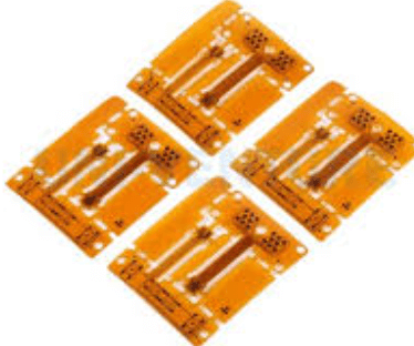
For instance, flexible PCBs may require materials that can withstand bending and flexing without degrading performance, while rigid PCBs may prioritize materials that offer structural support and durability.
In conclusion, the selection of materials for high frequency PCB design is a multifaceted process that requires careful consideration of various electrical, thermal, and mechanical properties. By understanding and prioritizing these factors, designers can ensure that their PCBs meet the demanding requirements of high frequency applications, ultimately leading to enhanced performance and reliability. As technology continues to advance, staying informed about the latest material innovations and their implications for high frequency design will be essential for engineers striving to push the boundaries of what is possible in the world of electronics.

Key Layout Techniques for High Frequency PCB Performance
In the realm of high-frequency printed circuit board (PCB) design, achieving optimal performance hinges on a meticulous understanding of key layout techniques.
As electronic devices continue to evolve, operating at increasingly higher frequencies, the demand for precise PCB design becomes paramount.
High-frequency PCBs are integral to applications such as radio frequency (RF) communication, microwave circuits, and advanced computing systems. Therefore, adhering to specific design rules is essential to mitigate issues such as signal integrity, electromagnetic interference (EMI), and thermal management.
To begin with, one of the fundamental aspects of high-frequency PCB design is the management of signal integrity.
Signal integrity refers to the preservation of the quality of electrical signals as they traverse the PCB. At high frequencies, signals are more susceptible to distortion, which can lead to data loss or corruption. To address this, designers must carefully consider trace geometry. The width, length, and spacing of traces should be optimized to minimize impedance mismatches and reflections. Utilizing controlled impedance traces, often achieved through microstrip or stripline configurations, is a common practice. These configurations help maintain consistent impedance, thereby reducing signal degradation.
Moreover, the choice of materials plays a crucial role in high-frequency PCB performance.
The dielectric constant and loss tangent of the substrate material significantly impact signal propagation. Low-loss materials, such as PTFE-based laminates, are preferred for high-frequency applications due to their ability to minimize signal attenuation. Additionally, the use of high-quality copper with smooth surface finishes can further enhance signal transmission by reducing skin effect losses.
Transitioning to another critical consideration, the layout of power and ground planes is vital for minimizing electromagnetic interference.
High-frequency circuits are particularly prone to EMI, which can disrupt the operation of sensitive components. To mitigate this, designers should implement solid ground planes that provide a low-impedance return path for signals. This not only reduces EMI but also enhances signal integrity by minimizing ground bounce and voltage fluctuations. Furthermore, the strategic placement of decoupling capacitors near power pins can help stabilize voltage levels and filter out high-frequency noise.
Thermal management is another key aspect that cannot be overlooked in high-frequency PCB design.
As frequencies increase, so does the potential for heat generation, which can adversely affect component performance and reliability. Effective thermal management techniques, such as the use of thermal vias and heat sinks, are essential to dissipate heat efficiently. Additionally, careful component placement can aid in distributing heat evenly across the PCB, preventing localized hotspots.
In addition to these technical considerations, collaboration between design and manufacturing teams is crucial to ensure that the PCB can be fabricated and assembled without compromising performance.
Design for manufacturability (DFM) principles should be integrated early in the design process to address potential challenges related to high-frequency operation. This includes considerations such as layer stack-up, via design, and solder mask application.
In conclusion, high-frequency PCB design demands a comprehensive approach that encompasses signal integrity, material selection, EMI mitigation, and thermal management. By adhering to these key layout techniques, designers can achieve PCBs that not only meet the stringent requirements of high-frequency applications but also ensure reliable and efficient performance. As technology continues to advance, the importance of mastering these design rules will only grow, underscoring the need for ongoing education and adaptation in the field of PCB design.

Signal Integrity Considerations in High Frequency PCB Design
In the realm of high frequency PCB design, signal integrity emerges as a critical consideration that can significantly impact the performance and reliability of electronic systems. As frequencies increase, the behavior of signals on a printed circuit board becomes more complex, necessitating a thorough understanding of various design rules to ensure optimal functionality. One of the primary challenges in high frequency PCB design is minimizing signal loss and distortion, which can be exacerbated by factors such as impedance mismatches, crosstalk, and electromagnetic interference.
To begin with, impedance control is paramount in maintaining signal integrity.
At high frequencies, even minor deviations in impedance can lead to reflections, which degrade signal quality. Therefore, designers must carefully calculate and maintain consistent impedance throughout the signal path. This involves selecting appropriate materials with known dielectric properties and using precise trace geometries. Additionally, the use of controlled impedance traces, such as microstrip or stripline configurations, can help achieve the desired impedance levels.
Moreover, crosstalk, which occurs when signals on adjacent traces interfere with each other, poses a significant threat to signal integrity in high frequency designs.
To mitigate crosstalk, designers should consider increasing the spacing between traces and employing ground planes to provide effective isolation. Furthermore, routing high-speed signals on different layers or at right angles can reduce the likelihood of crosstalk. It is also beneficial to use differential signaling, which inherently reduces susceptibility to crosstalk and electromagnetic interference.
In addition to crosstalk, electromagnetic interference (EMI) is another critical factor that can compromise signal integrity.
High frequency signals can radiate electromagnetic energy, potentially affecting nearby components and systems. To address this, designers should implement proper shielding techniques, such as using ground planes and metal enclosures, to contain electromagnetic emissions. Additionally, incorporating decoupling capacitors near power supply pins can help suppress high-frequency noise and stabilize power delivery.
Transitioning to the topic of signal routing, it is essential to minimize the length of high-speed traces to reduce signal delay and attenuation.
Shorter traces not only decrease the potential for signal degradation but also help maintain synchronization between signals. When longer traces are unavoidable, designers should consider using serpentine routing to equalize trace lengths and maintain timing integrity. Furthermore, avoiding sharp bends in traces is crucial, as these can introduce impedance discontinuities and reflections.
Another important aspect of high frequency PCB design is the selection of appropriate materials.
The choice of substrate material can significantly influence signal integrity, as different materials exhibit varying dielectric constants and loss tangents. Low-loss materials are preferred for high frequency applications, as they minimize signal attenuation and dispersion. Additionally, the use of low-profile copper can reduce skin effect losses, which become more pronounced at higher frequencies.
Finally, it is imperative to conduct thorough simulations and testing to validate the design and ensure signal integrity.
Simulation tools can model the behavior of high frequency signals and identify potential issues before physical prototyping. Once the PCB is fabricated, testing with high-speed oscilloscopes and network analyzers can verify that the design meets the required performance specifications.
In conclusion, maintaining signal integrity in high frequency PCB design requires a comprehensive approach that encompasses impedance control, crosstalk mitigation, EMI management, careful signal routing, material selection, and rigorous testing. By adhering to these design rules, engineers can ensure that their high frequency PCBs deliver reliable and efficient performance in increasingly demanding applications.

Best Practices for Via Design in High Frequency PCBs
In the realm of high frequency printed circuit board (PCB) design, the meticulous consideration of via design is paramount to ensuring optimal performance and signal integrity. Vias, which are the conductive pathways that connect different layers of a PCB, play a crucial role in the transmission of high-frequency signals. As frequencies increase, the impact of vias on signal integrity becomes more pronounced, necessitating a set of best practices to mitigate potential issues.
To begin with, understanding the electrical characteristics of vias is essential.
Vias introduce inductance and capacitance into the circuit, which can adversely affect signal integrity at high frequencies. Therefore, minimizing via inductance is a primary objective. One effective strategy is to reduce the via stub length. Via stubs, which are the unused portions of a via, can act as resonant structures that degrade signal quality. By back-drilling or using blind and buried vias, designers can significantly reduce stub lengths, thereby minimizing their impact on high-frequency signals.
Moreover, the choice of via size and shape is another critical consideration.
Smaller vias, often referred to as microvias, are preferable in high-frequency applications due to their lower parasitic inductance and capacitance. However, the mechanical strength and manufacturability of microvias must also be taken into account. Balancing these factors requires careful collaboration with PCB manufacturers to ensure that the chosen via design meets both electrical and structural requirements.
In addition to size, the placement of vias is equally important.
Vias should be strategically placed to minimize their impact on signal paths. For instance, placing vias directly in the path of a high-speed signal trace can introduce reflections and impedance discontinuities. To avoid this, designers should aim to place vias at locations where they have the least impact on signal integrity, such as at the ends of traces or in areas where signal paths are less critical.
Furthermore, the use of via stitching and via fences can enhance the performance of high-frequency PCBs.
Via stitching involves placing multiple vias around a signal trace to provide a low-inductance return path for high-frequency currents. This technique is particularly beneficial in reducing electromagnetic interference (EMI) and improving signal integrity. Similarly, via fences, which are rows of vias placed along the edges of a PCB, can help contain electromagnetic fields and prevent them from radiating into adjacent circuits.
Transitioning to the topic of via materials, it is important to select materials that are compatible with high-frequency applications.
The dielectric material surrounding the via can affect its electrical properties, so choosing a material with a low dielectric constant and low loss tangent is advisable. This choice helps to minimize signal attenuation and maintain signal integrity across the frequency spectrum.
Finally, simulation and testing are indispensable components of the via design process.
Advanced simulation tools can model the electrical behavior of vias and predict their impact on signal integrity. By simulating different via configurations, designers can identify potential issues and optimize their designs before fabrication. Once the PCB is manufactured, thorough testing should be conducted to verify that the via design meets the desired performance criteria.
In conclusion, the design of vias in high-frequency PCBs requires a comprehensive approach that considers electrical characteristics, size, placement, materials, and testing. By adhering to these best practices, designers can ensure that their high-frequency PCBs deliver reliable performance and maintain signal integrity in demanding applications.
