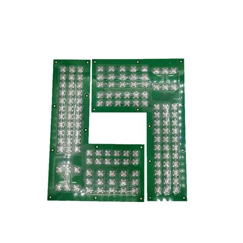
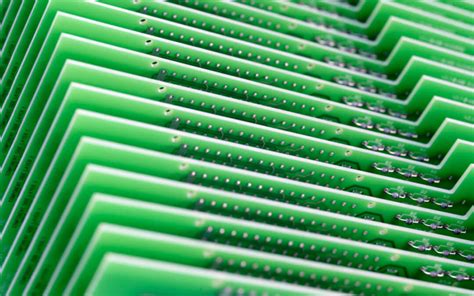
High frequency circuit pcb
Designing High Frequency Circuit PCBs: Best Practices and Tips
Designing high frequency circuit PCBs requires a meticulous approach to ensure optimal performance and reliability. As electronic devices continue to evolve, the demand for high frequency circuits has increased, necessitating a deeper understanding of the intricacies involved in their design. The process begins with selecting the appropriate materials, as the dielectric properties of the substrate can significantly impact signal integrity. Materials such as Rogers or Teflon are often preferred due to their low dielectric constant and minimal signal loss, which are crucial for maintaining signal fidelity at high frequencies.
Transitioning from material selection to layout design, it is essential to consider the impedance control of the traces.
Impedance mismatches can lead to signal reflections, which degrade the performance of high frequency circuits. To mitigate this, designers must carefully calculate the trace width and spacing, taking into account the dielectric constant of the substrate and the thickness of the copper. Utilizing simulation tools can aid in predicting the impedance and making necessary adjustments before the physical prototype is developed.
Moreover, the placement of components plays a pivotal role in high frequency PCB design.
Components should be positioned to minimize the length of high frequency signal paths, thereby reducing potential losses and interference. Additionally, grounding is a critical aspect that cannot be overlooked. A well-designed ground plane can provide a return path for signals, reducing electromagnetic interference (EMI) and enhancing signal integrity. It is advisable to use a continuous ground plane and avoid splitting it, as discontinuities can introduce unwanted inductance and capacitance.
In addition to grounding, the use of vias must be judiciously managed.
Vias introduce inductance, which can be detrimental at high frequencies. Therefore, minimizing the number of vias and ensuring they are placed strategically can help maintain signal quality. When vias are necessary, using multiple smaller vias instead of a single large one can reduce inductance and improve performance.
Furthermore, power distribution is another critical consideration in high frequency PCB design.
Ensuring a stable power supply to all components is vital, and this can be achieved by using power planes and decoupling capacitors. Decoupling capacitors should be placed as close as possible to the power pins of the components to filter out noise and provide a stable voltage level.
Thermal management is also an important factor, as high frequency circuits can generate significant heat.
Effective thermal management strategies, such as using thermal vias, heat sinks, and proper airflow, can prevent overheating and ensure the longevity of the circuit.
Finally, testing and validation are indispensable steps in the design process. Prototyping and testing the PCB under real-world conditions can reveal potential issues that were not apparent during the design phase. Iterative testing allows for refinements and adjustments, ensuring that the final product meets the desired specifications.
In conclusion, designing high frequency circuit PCBs is a complex task that requires careful consideration of various factors, from material selection to layout design and thermal management. By adhering to best practices and leveraging advanced simulation tools, designers can create high frequency PCBs that deliver superior performance and reliability. As technology continues to advance, staying informed about the latest developments and techniques in PCB design will be essential for success in this ever-evolving field.
Material Selection for High Frequency Circuit PCBs
When designing high frequency circuit printed circuit boards (PCBs), the selection of materials plays a crucial role in determining the performance and reliability of the final product. As electronic devices continue to evolve, operating at increasingly higher frequencies, the demand for PCBs that can support these frequencies without compromising signal integrity has become more pronounced. Consequently, understanding the properties and implications of various materials is essential for engineers and designers working in this field.
To begin with, one of the primary considerations in material selection for high frequency PCBs is the dielectric constant (Dk).
The dielectric constant affects the speed at which signals propagate through the material. Materials with a lower dielectric constant are generally preferred for high frequency applications because they allow signals to travel faster, reducing signal delay and improving overall performance. Additionally, a consistent dielectric constant across a range of frequencies is desirable to ensure stable performance. Materials such as PTFE (polytetrafluoroethylene) and certain ceramic-filled laminates are often chosen for their low and stable dielectric constants.
In addition to the dielectric constant, the dissipation factor (Df) is another critical parameter.
The dissipation factor measures the dielectric losses in the material, which can lead to signal attenuation and heat generation. For high frequency applications, materials with a low dissipation factor are preferred as they minimize energy loss and maintain signal integrity. This is particularly important in applications such as RF and microwave circuits, where even small losses can significantly impact performance. PTFE-based materials, again, are favored for their low dissipation factors, making them suitable for these demanding applications.
Thermal management is another important aspect to consider when selecting materials for high frequency PCBs.
As frequencies increase, so does the potential for heat generation, which can affect both the performance and longevity of the circuit. Materials with good thermal conductivity can help dissipate heat more effectively, preventing hotspots and ensuring reliable operation. Copper-clad laminates with enhanced thermal properties are often employed to address these concerns, providing a balance between electrical performance and thermal management.
Moreover, the mechanical properties of the material should not be overlooked.
High frequency PCBs often require precise manufacturing processes, and materials that offer dimensional stability and ease of fabrication are advantageous. This ensures that the intricate designs necessary for high frequency circuits can be accurately produced without warping or deformation. Materials that combine mechanical robustness with favorable electrical properties, such as certain glass-reinforced laminates, are frequently utilized in these scenarios.
Furthermore, cost considerations also play a role in material selection.
While high-performance materials like PTFE offer excellent electrical properties, they can be more expensive than traditional FR-4 materials. Therefore, designers must weigh the benefits of advanced materials against budget constraints, often opting for a compromise that meets both performance requirements and cost-effectiveness.
In conclusion, selecting the appropriate materials for high frequency circuit PCBs involves a careful evaluation of several factors, including dielectric constant, dissipation factor, thermal management, mechanical properties, and cost. By understanding and balancing these considerations, engineers can design PCBs that not only meet the demands of high frequency applications but also ensure reliability and efficiency. As technology continues to advance, the importance of informed material selection will only grow, underscoring its critical role in the development of cutting-edge electronic devices.
Challenges in Manufacturing High Frequency Circuit PCBs
The manufacturing of high frequency circuit printed circuit boards (PCBs) presents a unique set of challenges that require specialized knowledge and techniques to overcome. As electronic devices continue to evolve, the demand for high frequency circuits has increased, necessitating advancements in PCB manufacturing processes.
One of the primary challenges in this domain is the selection of appropriate materials.
High frequency circuits require substrates with low dielectric constants and minimal loss tangents to ensure signal integrity and reduce electromagnetic interference. Traditional materials like FR-4 are often unsuitable for these applications, prompting manufacturers to explore alternatives such as PTFE-based laminates or ceramic-filled substrates. These materials, while effective, can be more expensive and difficult to handle, adding complexity to the manufacturing process.
In addition to material selection, the precision of the manufacturing process is crucial.
High frequency circuits are highly sensitive to variations in trace width, spacing, and thickness. Even minor deviations can lead to significant performance issues, such as signal loss or impedance mismatches. Therefore, manufacturers must employ advanced fabrication techniques, such as laser direct imaging and precision etching, to achieve the necessary accuracy. These techniques, however, require significant investment in equipment and expertise, which can be a barrier for smaller manufacturers.
Moreover, the miniaturization of electronic components further complicates the manufacturing of high frequency PCBs.
As devices become smaller, the density of components on a PCB increases, necessitating more intricate designs and tighter tolerances. This miniaturization demands advanced design software capable of handling complex layouts and simulations to predict the behavior of high frequency signals. Additionally, the assembly process must be meticulously controlled to prevent defects that could compromise the performance of the circuit.
Thermal management is another critical challenge in the manufacturing of high frequency circuit PCBs.
High frequency signals can generate significant heat, which, if not properly managed, can lead to component failure or reduced performance. Manufacturers must incorporate effective thermal management solutions, such as heat sinks or thermal vias, into their designs. This requires a careful balance between thermal performance and electrical characteristics, as some thermal management techniques can adversely affect signal integrity.
Furthermore, the testing and quality assurance of high frequency PCBs are more demanding than those for standard PCBs.
Traditional testing methods may not be sufficient to detect issues specific to high frequency circuits, such as crosstalk or signal distortion. As a result, manufacturers must invest in specialized testing equipment and develop rigorous testing protocols to ensure the reliability and performance of their products. This not only increases the cost of production but also extends the time required to bring a product to market.
In conclusion, the manufacturing of high frequency circuit PCBs is fraught with challenges that require a combination of advanced materials, precise fabrication techniques, and rigorous testing procedures. As the demand for high frequency applications continues to grow, manufacturers must continually adapt and innovate to meet these challenges. While this can be a daunting task, it also presents opportunities for those who can successfully navigate the complexities of high frequency PCB manufacturing, ultimately leading to the development of more advanced and reliable electronic devices.
Signal Integrity in High Frequency Circuit PCB Design
Signal integrity is a critical consideration in the design of high frequency circuit printed circuit boards (PCBs). As electronic devices continue to evolve, the demand for faster processing speeds and higher data rates has led to the proliferation of high frequency circuits. These circuits, operating at gigahertz frequencies, present unique challenges that must be addressed to ensure optimal performance and reliability. Understanding the principles of signal integrity in high frequency circuit PCB design is essential for engineers and designers aiming to create efficient and effective electronic systems.
One of the primary concerns in high frequency circuit PCB design is the minimization of signal loss.
At high frequencies, signals are more susceptible to attenuation, which can degrade performance. To mitigate this, designers must carefully select materials with low dielectric loss and ensure that the PCB layout minimizes impedance discontinuities. The choice of substrate material, such as Rogers or Teflon, can significantly impact signal integrity by reducing dielectric losses and maintaining consistent impedance throughout the circuit.
Moreover, the physical layout of the PCB plays a crucial role in maintaining signal integrity.
As frequencies increase, the wavelength of the signals decreases, making them more sensitive to variations in trace geometry and spacing. Therefore, maintaining consistent trace widths and spacing is vital to prevent impedance mismatches that can lead to signal reflections and loss. Additionally, the use of controlled impedance traces, which are designed to have a specific impedance value, helps in minimizing signal reflections and ensuring that signals propagate smoothly across the board.
In addition to trace geometry, the placement of components on the PCB is another factor that influences signal integrity.
Components should be strategically placed to minimize the length of signal paths, thereby reducing the potential for signal degradation. Furthermore, the use of ground planes is essential in high frequency circuit PCB design. Ground planes provide a return path for signals, reducing electromagnetic interference (EMI) and crosstalk between adjacent traces. By providing a low-inductance path for return currents, ground planes help maintain signal integrity and improve overall circuit performance.
Transitioning from layout considerations to the importance of power integrity, it is crucial to ensure that power delivery networks (PDNs) are designed to support high frequency operation.
PDNs must be capable of delivering clean and stable power to all components on the PCB. This involves minimizing voltage fluctuations and noise, which can adversely affect signal integrity. Decoupling capacitors, strategically placed near power pins, help in filtering out high-frequency noise and maintaining a stable power supply.
Furthermore, the use of simulation tools is indispensable in high frequency circuit PCB design.
These tools allow designers to model and analyze the behavior of signals within the PCB, identifying potential issues before physical prototypes are built. By simulating signal propagation, impedance matching, and EMI, designers can optimize the PCB layout to enhance signal integrity and ensure reliable performance.
In conclusion, maintaining signal integrity in high frequency circuit PCB design is a multifaceted challenge that requires careful consideration of material selection, layout design, component placement, and power integrity. By addressing these factors, designers can create PCBs that support high frequency operation while minimizing signal loss and degradation. As technology continues to advance, the principles of signal integrity will remain a cornerstone of high frequency circuit PCB design, ensuring that electronic systems meet the demands of modern applications.