Essential Guide to Creation and Assembly of PCBs
Key Takeaways
In the creation and assembly of printed circuit boards (PCBs), there are several pivotal aspects that every electronic project developer should keep in mind. First and foremost, understanding the intricacies of pcb assembly is crucial, as it directly affects the performance and reliability of the final product. Each stage, from designing effective PCB layouts to selecting the appropriate materials, plays a significant role in achieving optimal performance for your project. Utilizing proper pcba techniques ensures that components are securely attached and aligned, which is essential for avoiding issues during operation. Furthermore, employing best practices throughout the process fosters excellence; this includes effective soldering techniques and ensuring cleanliness during assembly to prevent defects. Common challenges encountered in pcb assembly, such as misalignment or soldering flaws, can often be remedied with thorough troubleshooting strategies, so staying vigilant can save time and resources later on. Ultimately, quality control measures are paramount to ensure each PCB functions as intended before moving forward to testing—this guarantees your electronic innovations meet both safety standards and customer expectations.
Introduction to PCB Basics
Printed Circuit Boards (PCBs) are the backbone of modern electronics, playing a crucial role in connecting various electronic components. Understanding the fundamentals of pcb assembly is essential for anyone involved in electronic project development. A PCB serves as both a physical support and an electrically conductive pathway for components, ensuring that signals are efficiently transmitted. The process of pcba involves several stages, from initial design to final assembly.
It is important to recognize that the creation of a PCB starts with a well-thought-out design. Utilizing appropriate materials and tools is critical in this process; components must be selected carefully to match the power and performance requirements of the circuit. For new designers, it is advisable to invest time in familiarizing oneself with PCB design software and simulation tools, which can help visualize how the pcb assembly will function before actual production begins.
Moreover, attention to detail during the assembly phase can significantly influence the quality and reliability of the final product. Pay close heed to soldering techniques, ensuring that connections are solid and free from defects which could lead to future failures. Following strict guidelines during assembly not only enhances product reliability but also promotes efficient troubleshooting when issues arise.
“A well-assembled PCB today prevents countless headaches tomorrow.”
In summary, mastering these basic aspects of PCBs lays a solid foundation for successful electronic projects. Understanding how design, materials, and assembly techniques intertwine will help foster better practices as one advances in this field.
The Design Process: Creating Effective PCB Layouts
The design process is a critical phase in ensuring that your PCB functions as intended. A well-conceived layout can minimize interference and optimize performance, making it essential to focus on several key elements during this stage. First, begin by defining your circuit requirements; this will serve as the blueprint for your layout. Utilizing schematic capture software can significantly enhance clarity and precision, so consider tools that enable easy transition from schematic design to PCB assembly.
A crucial aspect of designing effective layouts is the arrangement of components. It’s essential to position high-frequency components closer to minimize signal loss and delay. Implementing a solid ground plane and ensuring proper power distribution are also critical steps that impact the overall performance of your pcba.
Important Layout Considerations:
| Factor | Description |
|---|---|
| Component Placement | Position components based on signal flow and function |
| Signal Routing | Keep traces short; avoid sharp corners |
| Grounding | Use continuous ground planes for reduced electromagnetic interference |
| Layer Management | Optimize the number of layers needed for routing |
Once you have arranged the components and established your routing paths, review for any potential issues such as trace width that may not align with current requirements. Tools with design rule checks (DRC) will help identify these common errors before entering the pcb assembly phase. Remember that thorough simulation and testing during this layout process can save significant time and costs later in the project development cycle.
The final layout should not only be functional but also efficient in terms of manufacturing processes and cost-effectiveness. A well-executed design is an integral step toward high-quality results in your electronic projects, paving the way for a successful transition into assembly and production stages.
Materials and Tools Needed for PCB Creation
Creating a Printed Circuit Board (PCB) involves careful selection of materials and tools that are essential for both the design and assembly processes. The foundation of any successful PCB project starts with the right materials, including copper-clad laminate, which serves as the substrate. This laminate is coated with a thin layer of copper, crucial for the electrical connections. Additionally, other materials like solder mask and silkscreen ink are vital for protecting the conductive traces and providing labels on the board.
In terms of tools, a well-equipped workspace should feature a soldering iron for attaching components to the PCB during assembly. A digital multimeter is essential for testing circuits to ensure functionality. Furthermore, designers often utilize specialized software tools for designing layouts—this is where initial considerations take shape in creating an effective PCB layout.
For those engaging in pcb assembly, having access to a reliable quality control system can make all the difference in achieving high standards during production. Whether you’re delving into manual assembly or leveraging automated processes, investing in precision tools ensures accurate component placement and optimal soldering—key factors in producing a robust final product.
Ultimately, understanding your project needs will help you make informed decisions on both materials and tools necessary for successful PCB design and assembly. Establishing this strong foundation is crucial as it prepares you for achieving high-quality results in your electronic projects.
Step-by-Step Guide to PCB Assembly Techniques
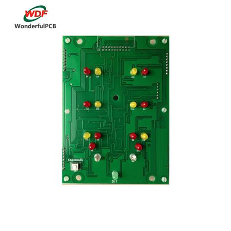
PCB assembly, often referred to as PCBA, is a critical phase in the development of electronic projects. This process involves several meticulous steps that ensure the successful integration of components onto the printed circuit board. To begin with, it is important to prepare your workspace and gather all necessary tools, such as soldering irons, tweezers, and magnifying lenses. A clean and organized environment is crucial for preventing mistakes during assembly.
Once you have everything in place, the first step in pcb assembly is to double-check your design schematic against the actual PCB layout. This helps to confirm that all components will fit correctly and are positioned as intended. Next, placing the components on the board according to their designated spots is essential. Utilization of tweezers can aid in positioning small parts accurately without risking damage.
After component placement, it’s time for soldering. Proper soldering techniques should be employed to avoid short circuits or weak connections; this step often determines the quality of your finished product. Ensure that each solder joint is clean and shiny, which indicates a solid bond between component leads and PCB pads.
Following soldering, inspection plays a vital role in pcb assembly. Utilize visual inspection or even automated systems if available to identify any potential issues before proceeding further. Finally, thorough testing after assembly will validate the functionality of your assembled PCB and ensure it meets project specifications.
By adhering to these detailed steps during your PCBA process, you can significantly enhance your chances of achieving high-quality results in your electronic project development endeavors.
Best Practices for Achieving High-Quality Results
Achieving high-quality results in pcb assembly (PCBA) involves adherence to several best practices that can significantly enhance the performance and reliability of your electronic projects. First and foremost, preparation is key. Ensuring that the PCB design is optimized and free of errors before assembly is crucial. This can include verifying the schematic against the layout, checking for design rule violations, and performing a thorough simulation if applicable.
Next, using high-quality materials cannot be understated; selecting the right substrate, solder paste, and components can prevent many common issues during assembly. During the assembly process, maintaining a clean working environment is essential to avoid contamination that could affect solder joints. It is recommended to use appropriate tools, such as automatic pick-and-place machines for accuracy and consistency in component placement.
Additionally, implementing proper soldering techniques—whether using hand soldering or automated methods—ensures strong electrical connections. Monitoring parameters like temperature during soldering can help achieve optimal coverage with minimal defects. Furthermore, conducting regular checks during assembly allows for early detection of potential problems, which can lead to improved outcomes.
Last but not least, after completing the pcb assembly, consider rigorous testing methodologies such as continuity tests and functional tests. This step confirms that all connections are solid and that the assembled PCB performs as intended in its operating environment. By following these best practices, you can achieve a high-quality PCBA that not only meets but exceeds expectations in electronic project development.
Troubleshooting Common PCB Assembly Issues
When working on pcb assembly, encountering issues is often inevitable. Understanding these common problems can significantly enhance the efficiency of the assembly process. One frequent issue is misalignment of components. This typically occurs during soldering when components are not placed accurately on the PCB. Ensuring that you use proper alignment tools and techniques is vital for achieving a successful pcb assembly. Another common challenge is cold solder joints, which can lead to unreliable connections. This usually happens when the solder doesn’t flow adequately around the component lead and pad, often due to insufficient heating or a lack of solder. To avoid this, it’s crucial to maintain appropriate soldering temperatures and techniques.
Additionally, contamination on the surface of the PCB can result in poor soldering quality, leading to defects in the final product. Maintaining a clean work environment and properly storing your materials can mitigate this issue. Furthermore, component placement errors during initial assembly can lead to complications in functionality later on. Verifying your pcba layouts against schematics before beginning assembly helps in catching potential mistakes early.
Ultimately, addressing these troublesome areas requires diligence and attention to detail throughout the pcb assembly process. By being proactive about these common issues, you can enhance both the quality and reliability of your electronic projects while ensuring a smoother development process overall.

Finalizing Your Project: Testing and Quality Control
Once the pcb assembly is complete, the next crucial step is to ensure your project is functioning as intended. Testing your assembled printed circuit board (PCB) involves a series of systematic procedures designed to identify potential issues and confirm that all connections are secure. Begin with a visual inspection of the pcba for any solder bridges, misaligned components, or other physical anomalies. After this initial check, employ multimeters and oscilloscopes to perform electrical tests; these tools will help assess the integrity of the circuit paths and ensure voltage levels conform to specifications.
It is also imperative to conduct functionality tests that simulate actual operating conditions. This process can help identify intermittent failures that might not be apparent during standard inspections. Moreover, keeping documentation of the testing results allows for accountability and can be valuable if modifications or enhancements are necessary in the future.
Incorporating a structured quality control process increases confidence in the reliability of your pcb assembly. If discrepancies arise during testing, revisiting earlier steps may be required, such as re-evaluating design parameters or component selection. Consistent adherence to best practices in both assembly and testing phases will ultimately contribute to achieving high-quality results in your electronic project development.

Future Trends in PCB Technology and Assembly Techniques
As the demand for advanced electronics continues to rise, pcb assembly and associated manufacturing processes are undergoing significant innovations. One notable trend is the integration of automated technologies in the pcba sector, enhancing both efficiency and precision. Automation minimizes human error in assembly, leading to higher-quality products. Additionally, the adoption of flexible printed circuit boards (FPCBs) is on the rise, providing greater versatility and enabling designs that conform to various spatial constraints. The push for miniaturization in electronics parallels advancements in assembly techniques, allowing for more compact devices without sacrificing performance. Furthermore, as sustainability becomes paramount, many companies are exploring eco-friendly materials and production methods that reduce waste during the pcb creation process. This shift not only aligns with global environmental goals but also meets client expectations for responsible manufacturing practices. Overall, these trends indicate a promising future for pcb assembly and underscore the importance of continuous adaptation in this rapidly evolving field.
Conclusion
In summary, understanding the intricate processes involved in PCB assembly is essential for the successful development of electronic projects. This guide has provided a comprehensive overview of the various stages involved in the creation and assembly of PCBs. From selecting the appropriate materials to employing effective techniques, every step plays a crucial role in achieving high-quality results. By following best practices and being mindful of common pitfalls during PCBA, practitioners can enhance their skills and ensure the reliability of their final products. The importance of rigorous testing and quality control cannot be overstated, as it significantly impacts both functionality and durability. As technology continues to evolve, staying informed about emerging trends in PCB fabrication will empower designers to adopt innovative solutions that cater to modern demands.
FAQs
What is PCB assembly?
PCB assembly, often referred to as PCBA, is the process of connecting electronic components to a printed circuit board (PCB) to create a functional electronic device.
Why is the PCB assembly process important?
The PCB assembly process is crucial because it directly affects the performance and reliability of electronic products. High-quality assembly ensures that connections between components are robust, reducing the risk of failure.
What are the common methods used in PCB assembly?
There are several common methods for PCB assembly, including manual soldering, automated pick-and-place machines, and wave soldering techniques. Each method has its own advantages and is chosen based on the specific requirements of the project.
What components are typically used in PCB assembly?
Components used in PCBA can range from resistors and capacitors to integrated circuits and connectors. The choice of components depends on the intended functionality of the final product.
How can I ensure a high-quality PCB assembly?
To achieve high-quality results in PCB assembly, it is essential to follow best practices during both design and manufacturing stages. This includes proper layout design, selecting high-quality materials, and adhering to strict quality control measures throughout the process.
What are some common issues encountered during PCB assembly?
Common issues include misalignment of components, cold solder joints, and insufficient solder. Understanding these problems can help in troubleshooting and preventing them during production.
For more detailed information on how to enhance your understanding or improve your skills in pcb assembly, please click here: Learn More About PCB Assembly