Custom PCB Printing and Assembly Solutions for Your Projects
Key Takeaways
Custom PCB printing and assembly serve as fundamental components in the development of electronic devices. Understanding the intricacies of pcb assembly can significantly influence the overall performance and reliability of a product. When opting for pcba services, one can benefit from a range of tailored solutions designed specifically for diverse project needs. This includes various design specifications that accommodate unique project requirements while maintaining optimal functionality. Moreover, leveraging advanced techniques in custom PCB printing can result in improved precision, allowing designers to push the limits of innovation. The selection of appropriate materials also plays a crucial role in achieving the desired performance metrics. Furthermore, incorporating stringent quality control measures throughout the pcb assembly process ensures that each unit meets high standards before reaching end-users. As industries increasingly shift towards customization, understanding these key takeaways will empower professionals to make informed decisions that enhance both product development and market success.
Understanding Custom PCB Printing: An Introduction
Custom PCB printing and assembly is a crucial aspect of electronics development, allowing engineers and designers to create tailored solutions for their specific project needs. At its core, pcb assembly involves a meticulous process where various electronic components are mounted onto a printed circuit board (PCB), ensuring efficient electrical connections. This process combines precision manufacturing techniques with a deep understanding of the unique requirements of each project.
Through innovations in pcba, companies can achieve greater flexibility in design, accommodating complex circuit layouts and more sophisticated components. As technology evolves, the methods used in custom PCB printing are also advancing, leading to improved efficiency and reduced production times. Moreover, selecting the right materials during the design phase is vital, as it can influence not only performance but also durability and cost-effectiveness.
“Embracing custom solutions in PCB design can significantly enhance your electronics development process.”
By recognizing the importance of quality control measures throughout production, industries can minimize errors and ensure that the final product meets rigorous standards. Ultimately, understanding this intricate process is essential for anyone looking to harness the full potential of custom PCB technology in their projects.
Advantages of Tailored PCB Design for Projects
In today’s fast-paced electronics industry, the necessity for custom PCB printing and assembly has become paramount. When engaging in electronic projects, opting for tailored PCB design can significantly enhance both functionality and performance. One of the primary advantages of a custom-designed PCB is the ability to meet specific project requirements, which often fosters innovative solutions not achievable with standard boards.
Tailored PCB assembly allows for greater design flexibility, enabling engineers to optimize the layout for space, signal integrity, and power efficiency. This customized approach ensures that every component placement is deliberate, reducing potential interference and enhancing overall product reliability.
Moreover, custom PCBs often result in streamlined production processes, which can be crucial for manufacturers with tight deadlines. By selecting appropriates materials and manufacturing techniques that align with the unique specifications of a project, companies can achieve significant cost efficiencies in both material usage and assembly time.
The following table illustrates the key benefits associated with tailored PCB design:
| Advantage | Description |
|---|---|
| Enhanced Functionality | Custom design allows optimization per project needs |
| Improved Efficiency | Space-saving layouts and reduced interference |
| Cost-effectiveness | Streamlined processes lead to lower production costs |
| Flexibility in Design | Ability to incorporate unique features easily |
In conclusion, understanding these advantages is crucial as they can lead to creating superior electronic products that not only meet but exceed market expectations. When combined with proficient PCBA, these customized solutions pave the way for successful outcomes in various projects across different sectors.
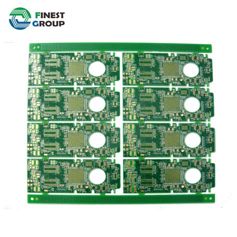
The Process of Custom PCB Assembly: A Step-by-Step Guide
The journey of custom PCB assembly (PCBA) begins with a well-structured plan that encompasses several crucial steps. First, the design phase is paramount, where engineers utilize advanced software to create detailed layouts of the circuit board. These layouts must consider component placement, electrical connections, and design rules to ensure efficiency and performance. Once the design is finalized, it is transformed into a physical representation through precision printing techniques that are essential for quality PCB assembly.
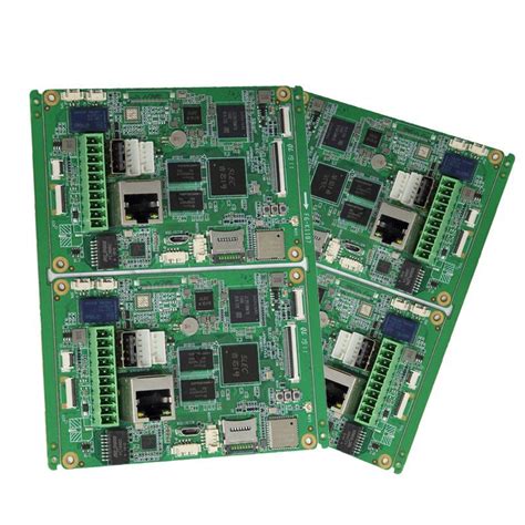
Next comes the sourcing of materials, which includes selecting the right substrates and components to ensure reliability and durability in the final product. The process then moves into manufacturing, where circuit boards are fabricated using state-of-the-art technology like surface mount technology (SMT) or through-hole assembly. Each method has its unique advantages, making it vital to choose according to project specifications.
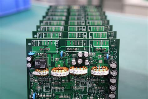
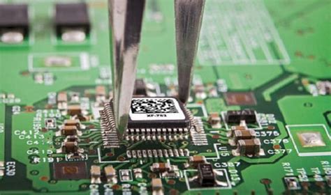
After fabrication, expert technicians meticulously assemble the PCBs, incorporating rigorous testing protocols at various stages. This diligent approach guarantees that every assembly meets high standards for functionality and quality control. By focusing on comprehensive testing methods throughout the process—from initial design to final assembly—developers can detect potential issues early on and rectify them proactively.
Ultimately, this step-by-step method not only improves efficiency but also enhances product reliability in competitive markets. As a result, organizations can confidently deliver high-quality electronics that align with their project goals, reinforcing their reputation in an ever-evolving industry landscape. Each step in the PCB assembly process contributes significantly to maximizing overall project success and ensuring satisfaction for end-users.
Innovations in PCB Manufacturing Techniques
The landscape of PCB manufacturing has evolved significantly, particularly with the emergence of advanced techniques that enhance both productivity and quality. Recent innovations have streamlined the pcb assembly process, allowing for faster turnaround times and lower costs while maintaining high standards. For instance, the integration of automated processes in pcba not only improves accuracy but also reduces human error in assembly. Additionally, advancements in 3D printing have opened up new possibilities for complex designs and rapid prototyping, enabling engineers to iterate more quickly on their projects. Companies are now exploring novel materials that can withstand higher thermal and electrical demands, thus enhancing performance over traditional options. Furthermore, implementing sophisticated software for design verification during the manufacturing stages ensures that every component is optimized for its intended application. Overall, these innovations are crucial in meeting the ever-increasing demands of diverse industries, ensuring that tailored solutions are viable and leading to enhanced product reliability and functionality.
Choosing the Right Materials for Your PCB Projects
When embarking on a printed circuit board (PCB) project, selecting the appropriate materials is essential for achieving optimal performance and reliability. The substrate material, often fiberglass or epoxy, plays a pivotal role in the integrity of the circuit. For example, FR-4 is a popular choice due to its balance of cost, availability, and electrical characteristics. Additionally, understanding the thermal properties of materials is crucial, especially if the PCB assembly will be subjected to varying temperatures during operation. By choosing materials that can withstand thermal cycling and mechanical stress, engineers can ensure that their designs remain functional over time.
Moreover, it is important to consider the conductivity of metals used in fabrication—copper is typically favored for its excellent electrical properties. Advances in custom printing technology now allow for high-precision tracks and finer pitches on PCBA, enabling more compact designs while maintaining performance. The functional requirements of your project should also be taken into account; whether you need flexibility or rigidity can influence your choices profoundly.
Lastly, selecting high-quality components during the assembly process can significantly impact overall project success. Components that are resilient to environmental conditions and high voltage can help avert future failure points in your pcb assembly operations. Integrating these considerations into your workflow ensures that you achieve not only design excellence but also long-term efficiency in your electronic applications.
Quality Control Measures in Custom PCB Production
In the realm of custom PCB printing and assembly, rigorous quality control measures are essential to ensure that each board meets the specific requirements and standards needed for successful project outcomes. The complexity of modern electronics necessitates a comprehensive approach to quality assurance that begins at the design phase and extends through to the final assembly of the PCB. Employing advanced techniques such as automated optical inspection (AOI) allows manufacturers to detect defects early in the production process, ensuring that any discrepancies in the patterns or components used are addressed promptly. Additionally, implementing stringent testing protocols, like in-circuit testing (ICT), is crucial for verifying the integrity of connections within a fully assembled PCBA. Such measures not only enhance reliability but also significantly reduce the likelihood of product failure in final applications. By maintaining a focus on continuous improvement through regular audits and feedback loops, manufacturers can uphold high standards that translate into superior functionality and durability. Overall, embracing these quality control strategies not only fortifies trust in custom PCB assembly services but also paves the way for innovative solutions tailored to meet diverse project needs effectively.
Case Studies: Successful Projects Using Custom PCBs
The use of custom PCB printing and assembly has revolutionized the landscape of electronics development, leading to a plethora of successful projects across various industries. One notable example is in the medical technology sector, where a company developed a portable health monitoring device that relied on PCB assembly to achieve compactness and functionality. By employing tailored pcba solutions, engineers were able to integrate multiple sensors and wireless communication modules onto a single board, enhancing performance while reducing production costs.
Another compelling case comes from the automotive industry, where an electric vehicle manufacturer utilized custom PCBs to optimize its battery management system. The intricate design enabled real-time monitoring and control of battery cells, essential for maximizing efficiency and safety. The precision achieved through specialized pcb assembly techniques allowed for faster prototyping and iteration cycles, facilitating quicker time-to-market for innovative features.
Similarly, in the consumer electronics sector, a startup launched a smart home device that showcased the versatility of custom PCBs in accommodating various wireless technologies while maintaining an aesthetic appearance. By carefully selecting materials and employing state-of-the-art manufacturing techniques in their pcba, they ensured reliable connectivity and durability in different environments.
These cases underline the significant role that custom PCBs play in driving technological advancements. The adaptability provided by custom solutions not only fuels innovation but also meets specific project requirements more efficiently. With ongoing advancements in manufacturing technologies and design methodologies, the future landscape for custom PCB printing and assembly holds even greater potential for diverse applications across various sectors.
Future Trends in Custom PCB Printing and Assembly
As technology continues to evolve, the world of custom PCB printing and assembly is on the brink of exciting developments that promise to enhance the way we approach electronic design and manufacturing. Notably, advancements in 3D printing technologies are poised to revolutionize the pcb assembly process, enabling faster prototyping and greater design flexibility. This method allows for intricate designs that were previously challenging to achieve with traditional techniques. Additionally, there is a growing emphasis on sustainability, leading manufacturers to explore eco-friendly materials that maintain high performance while reducing environmental impact.
Moreover, the integration of Internet of Things (IoT) technologies is reshaping how PCBs connect and interact within devices. Smart PCBs equipped with embedded sensors enhance functionality while providing real-time data for monitoring performance. The trend toward miniaturization means that pcba processes will increasingly focus on maximizing space efficiency without compromising on quality or reliability.
As industries demand shorter turnaround times, automation in custom PCB assembly processes is becoming essential. Automated systems not only speed up production but also improve accuracy and reduce human error. In summary, these trends are setting the stage for a new era in custom PCB printing and assembly, where innovation meets efficiency and quality performance rises to new heights.
Conclusion
Incorporating custom PCB printing and assembly solutions into your projects can significantly impact the efficiency and performance of your electronic designs. By embracing advanced pcb assembly techniques, you open the door to unparalleled levels of design flexibility and precision manufacturing. Each stage of the pcba process, from initial design conception to final assembly, is tailored to meet specific project requirements, ensuring that the end product aligns perfectly with your vision. Additionally, the use of high-quality materials enhances durability and functionality, allowing for innovative designs that can accommodate a wide range of applications. As you consider future projects, it is essential to recognize that choosing the right custom PCB solutions not only streamlines production but also contributes to overall project success. By adhering to strict quality control measures throughout the production process, you can ensure that every component meets high standards, thus fostering reliability in your electronics development journey. The future of custom PCB printing and assembly is bright, filled with advancements that promise even greater capabilities for designers and engineers alike.
FAQs
What is PCB assembly?
PCB assembly, or PCBA, is the process of soldering electronic components to a printed circuit board to create a functional electronic product. This process is crucial for transforming the design of a PCB into a market-ready device.
Why should I choose custom PCB printing?
Choosing custom PCB printing allows for greater design flexibility and the ability to meet specific project requirements. Tailored solutions can enhance efficiency and performance, ensuring that your project stands out in its functionality.
What are the typical materials used in PCBs?
Common materials for PCB assembly include FR-4, which is a standard material, as well as advanced options like flexible materials or high-frequency substrates. Selecting the right material can significantly impact the performance of your circuit board.
How is quality control maintained in custom PCB production?
Quality control measures include rigorous testing at various stages of production, which may involve visual inspections, automated optical inspections (AOI), and functional testing. These steps ensure that each PCBA meets defined standards before reaching clients.
What innovations are influencing PCB manufacturing techniques?
Technological innovations such as improved layered constructions, utilizing smaller component sizes, and advanced soldering techniques are currently influencing custom PCB printing and assembly. These developments lead to more compact designs and enhanced functionality.