High density interconnect pcb market
Growth Trends In The High Density Interconnect PCB Market
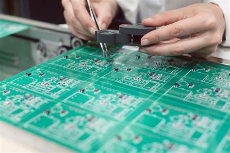
The high density interconnect (HDI) printed circuit board (PCB) market has been experiencing significant growth, driven by the increasing demand for miniaturized electronic devices and the rapid advancement of technology.
As consumer preferences shift towards more compact and efficient electronic products, manufacturers are compelled to innovate and adopt HDI PCBs, which offer enhanced performance and reliability.
This trend is further bolstered by the proliferation of smartphones, tablets, and wearable devices, all of which require sophisticated circuitry in a limited space.
One of the primary factors contributing to the growth of the HDI PCB market is the burgeoning consumer electronics sector.
With the global population becoming increasingly tech-savvy, there is a heightened demand for devices that are not only smaller but also more powerful. HDI PCBs, with their ability to support higher wiring density and finer lines and spaces, are ideally suited to meet these requirements.
Moreover, the integration of advanced features such as touch screens, high-resolution cameras, and augmented reality capabilities necessitates the use of HDI technology to accommodate the complex circuitry involved.
In addition to consumer electronics, the automotive industry is also playing a pivotal role in the expansion of the HDI PCB market.
The advent of electric vehicles (EVs) and autonomous driving technologies has led to a surge in demand for sophisticated electronic systems within vehicles.
HDI PCBs are crucial in this context, as they enable the integration of various electronic components in a compact form, thereby reducing the overall weight and improving the efficiency of the vehicle.
Furthermore, the increasing emphasis on safety and connectivity features in modern vehicles underscores the need for reliable and high-performance PCBs.
The telecommunications sector is another significant contributor to the growth of the HDI PCB market.
With the rollout of 5G networks and the subsequent increase in data transmission speeds, there is a pressing need for PCBs that can handle higher frequencies and greater data loads. HDI technology, with its ability to support high-speed signal transmission and reduce signal loss, is well-positioned to address these challenges. As a result, telecom companies are increasingly incorporating HDI PCBs into their infrastructure to enhance network performance and reliability.
Moreover, the medical industry is witnessing a growing adoption of HDI PCBs, driven by the demand for compact and portable medical devices.
As healthcare providers seek to offer more personalized and efficient care, there is a need for devices that can perform complex functions while remaining easy to use and transport. HDI PCBs facilitate the miniaturization of medical devices, enabling the development of advanced diagnostic and monitoring equipment that can be used in a variety of settings.
In conclusion, the high density interconnect PCB market is poised for continued growth, fueled by the increasing demand for miniaturized and high-performance electronic devices across various industries.
As technology continues to evolve, the need for sophisticated circuitry solutions will only intensify, further driving the adoption of HDI PCBs.
With their ability to support complex designs and enhance device functionality, HDI PCBs are set to play a crucial role in shaping the future of electronics. As such, stakeholders in the electronics manufacturing industry must remain attuned to these growth trends and invest in the development and production of HDI technology to stay competitive in this rapidly expanding market.
Key Technologies Driving High Density Interconnect PCB Innovations
The high density interconnect (HDI) printed circuit board (PCB) market is experiencing significant growth, driven by a confluence of technological advancements and increasing demand for miniaturized electronic devices.
As the electronics industry continues to evolve, HDI PCBs have emerged as a critical component in the design and manufacture of compact, high-performance products.
This evolution is largely attributed to several key technologies that are propelling innovations within the HDI PCB sector.
One of the primary technologies driving HDI PCB innovations is the development of advanced materials.
The use of high-performance laminates and substrates has enabled manufacturers to produce PCBs with superior thermal and electrical properties.
These materials are essential for supporting the increased circuit density and complexity required by modern electronic devices.
Moreover, the integration of materials with low dielectric constants and high thermal conductivity has facilitated the production of PCBs that can operate efficiently at higher frequencies, thereby enhancing the overall performance of electronic systems.
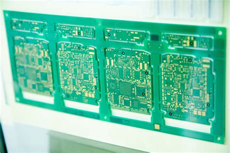
In addition to material advancements, the adoption of laser drilling technology has revolutionized the HDI PCB manufacturing process.
Laser drilling allows for the creation of microvias, which are small holes that connect different layers of a PCB.
This technology enables the production of PCBs with multiple layers and higher wiring density, which is crucial for accommodating the intricate designs of contemporary electronic devices. The precision and efficiency of laser drilling have significantly reduced the time and cost associated with PCB fabrication, making it a cornerstone of HDI PCB production.
Furthermore, the implementation of advanced design software has played a pivotal role in the innovation of HDI PCBs.
Modern design tools offer sophisticated simulation and modeling capabilities, allowing engineers to optimize PCB layouts for performance and manufacturability. These tools facilitate the integration of complex features such as blind and buried vias, which are essential for achieving the high interconnect density characteristic of HDI PCBs. By enabling more accurate and efficient design processes, advanced software solutions have accelerated the development of next-generation electronic products.
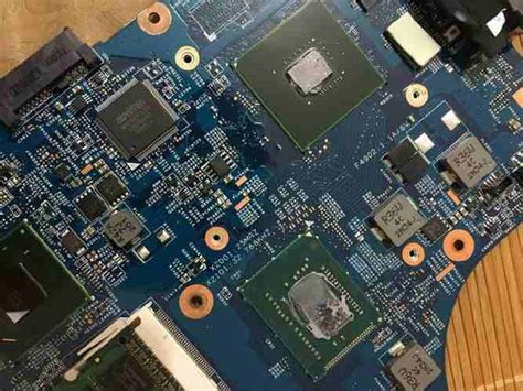
Another significant technological advancement is the use of surface mount technology (SMT) in HDI PCB assembly.
SMT allows for the placement of components directly onto the surface of the PCB, eliminating the need for through-hole connections. This technology supports the miniaturization of electronic devices by enabling the use of smaller components and reducing the overall footprint of the PCB. The combination of SMT with HDI technology has resulted in PCBs that are not only more compact but also more reliable and cost-effective.
Moreover, the rise of flexible and rigid-flex HDI PCBs has expanded the application possibilities for these advanced circuit boards.
Flexible PCBs offer the advantage of being able to bend and conform to various shapes, making them ideal for use in wearable technology and other applications where space is limited. Rigid-flex PCBs, which combine the benefits of both rigid and flexible circuits, provide enhanced durability and performance in demanding environments. These innovations have opened new avenues for the deployment of HDI PCBs across a wide range of industries.
In conclusion, the high density interconnect PCB market is being driven by a suite of key technologies that are enabling the production of smaller, more powerful, and more efficient electronic devices. From advanced materials and laser drilling to sophisticated design software and surface mount technology, these innovations are shaping the future of electronics manufacturing. As the demand for compact and high-performance devices continues to grow, the role of HDI PCBs in the electronics industry is set to become increasingly prominent.
Challenges And Opportunities In The High Density Interconnect PCB Industry
The high density interconnect (HDI) printed circuit board (PCB) market is experiencing a period of significant transformation, driven by rapid technological advancements and evolving consumer demands. As the industry continues to grow, it faces a unique set of challenges and opportunities that stakeholders must navigate to remain competitive. Understanding these dynamics is crucial for companies aiming to capitalize on the potential of HDI PCBs.
One of the primary challenges in the HDI PCB industry is the increasing complexity of electronic devices.
As consumer electronics, automotive systems, and industrial applications demand more compact and efficient designs, the need for advanced PCBs with higher component density and improved performance becomes paramount.
This complexity necessitates sophisticated manufacturing processes and cutting-edge materials, which can drive up production costs.
Consequently, companies must invest in research and development to innovate and refine their manufacturing techniques, ensuring they can produce high-quality HDI PCBs at competitive prices.
Moreover, the HDI PCB market is also grappling with supply chain disruptions, which have been exacerbated by global events such as the COVID-19 pandemic.
These disruptions have led to shortages of critical raw materials and components, resulting in increased lead times and production delays. To mitigate these risks, companies are exploring strategies such as diversifying their supplier base, investing in local production facilities, and adopting advanced inventory management systems.
By enhancing supply chain resilience, businesses can better navigate uncertainties and maintain a steady flow of products to meet market demand.
Despite these challenges, the HDI PCB industry is ripe with opportunities, particularly as the demand for miniaturized and high-performance electronic devices continues to surge.
The proliferation of technologies such as 5G, the Internet of Things (IoT), and artificial intelligence (AI) is driving the need for more sophisticated PCBs that can support higher data rates and increased functionality. This trend presents a significant growth opportunity for companies that can deliver innovative HDI solutions tailored to these emerging applications.
Furthermore, the push towards sustainability and environmental responsibility is opening new avenues for growth in the HDI PCB market.
As consumers and regulators increasingly prioritize eco-friendly products, there is a growing demand for PCBs that are manufactured using sustainable practices and materials. Companies that can demonstrate a commitment to reducing their environmental footprint are likely to gain a competitive edge, as they align with the values of environmentally conscious consumers and comply with stringent regulatory requirements.
In addition, the rise of smart manufacturing and Industry 4.0 technologies is transforming the HDI PCB production landscape.
By leveraging automation, data analytics, and machine learning, companies can enhance their production efficiency, reduce waste, and improve product quality. These advancements not only help in addressing the challenges of cost and complexity but also enable businesses to respond more swiftly to changing market demands.
In conclusion, the high density interconnect PCB market is at a pivotal juncture, characterized by both formidable challenges and promising opportunities.
Companies that can adeptly navigate the complexities of modern electronics, bolster their supply chain resilience, and embrace innovation and sustainability are well-positioned to thrive in this dynamic industry.
As the demand for advanced electronic devices continues to grow, the HDI PCB market will undoubtedly play a crucial role in shaping the future of technology.
Impact Of High Density Interconnect PCBs On Consumer Electronics
The high density interconnect (HDI) printed circuit board (PCB) market has been experiencing significant growth, driven largely by the increasing demand for more compact, efficient, and high-performance consumer electronics.
As technology continues to evolve, the role of HDI PCBs in the consumer electronics sector becomes increasingly pivotal. These advanced PCBs are characterized by their higher wiring density per unit area, which is achieved through the use of finer lines and spaces, smaller vias, and capture pads.
This allows for more components to be placed on both sides of the board, thereby enhancing the functionality and performance of electronic devices.
One of the primary impacts of HDI PCBs on consumer electronics is the facilitation of miniaturization.
As consumers demand sleeker, more portable devices, manufacturers are compelled to design products that are not only smaller but also more powerful.
HDI technology enables this by allowing for the integration of more components in a limited space without compromising on performance. This is particularly evident in smartphones, tablets, and wearable devices, where space is at a premium, and every millimeter counts.
The ability to pack more functionality into a smaller form factor has been a game-changer, enabling the development of devices that are not only compact but also feature-rich.
Moreover, HDI PCBs contribute significantly to the enhancement of performance in consumer electronics.
The increased interconnect density allows for faster signal transmission and improved electrical performance, which is crucial for high-speed applications.
This is particularly important in devices that require rapid processing and data transfer, such as gaming consoles and high-definition audio and video equipment.
The improved performance is not only a result of the increased density but also due to the use of advanced materials and manufacturing processes that reduce signal loss and interference.
In addition to miniaturization and performance enhancement, HDI PCBs also play a crucial role in improving the reliability and durability of consumer electronics.
The use of microvias and blind/buried vias in HDI designs reduces the number of layers required, which in turn decreases the complexity and potential points of failure in the PCB. This results in more robust devices that can withstand the rigors of daily use, thereby enhancing consumer satisfaction and brand loyalty.
Furthermore, the adoption of HDI PCBs aligns with the growing trend towards environmentally sustainable electronics.
The efficient use of materials and the reduction in size and weight of devices contribute to lower energy consumption during both the manufacturing process and the product’s lifecycle. This is increasingly important as consumers and manufacturers alike become more conscious of their environmental footprint.
In conclusion, the impact of high density interconnect PCBs on consumer electronics is profound and multifaceted. By enabling miniaturization, enhancing performance, improving reliability, and supporting sustainability, HDI technology is at the forefront of the evolution of consumer electronics.
As the demand for more advanced and efficient devices continues to rise, the role of HDI PCBs will undoubtedly become even more critical, driving innovation and shaping the future of the industry. The ongoing advancements in HDI technology promise to unlock new possibilities, further transforming the landscape of consumer electronics and meeting the ever-evolving needs of consumers worldwide.