High density interconnect (hdi) pcb
Advantages Of High Density Interconnect (HDI) PCB In Modern Electronics
High Density Interconnect (HDI) Printed Circuit Boards (PCBs) have emerged as a pivotal innovation in the realm of modern electronics, offering a multitude of advantages that cater to the ever-evolving demands of contemporary technology. As electronic devices continue to shrink in size while simultaneously increasing in functionality, the need for more efficient and compact circuit board solutions has become paramount.
HDI PCBs address this need by providing a platform that supports higher wiring density per unit area, thereby enabling the development of smaller, lighter, and more powerful electronic devices.
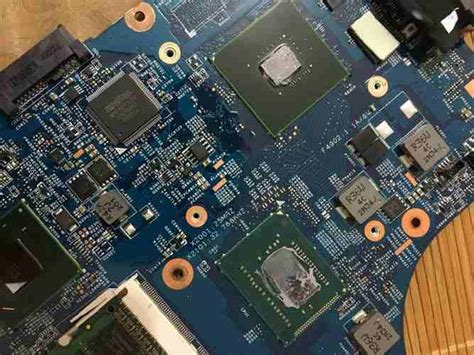
One of the primary advantages of HDI PCBs is their ability to accommodate a higher number of interconnections in a limited space.
This is achieved through the use of microvias, blind vias, and buried vias, which allow for more layers and finer lines and spaces. Consequently, HDI technology facilitates the integration of more components on a single board, which is particularly beneficial for devices such as smartphones, tablets, and wearable technology, where space is at a premium. The increased density of interconnections not only enhances the functionality of these devices but also contributes to their miniaturization, a key trend in the electronics industry.
Moreover, HDI PCBs offer improved electrical performance, which is crucial for high-speed and high-frequency applications.
The shorter signal paths and reduced parasitic effects associated with HDI designs result in lower signal loss and better signal integrity. This is particularly advantageous in applications such as telecommunications, aerospace, and automotive industries, where reliable and efficient signal transmission is essential.
Additionally, the enhanced thermal performance of HDI PCBs, due to their ability to dissipate heat more effectively, ensures the longevity and reliability of electronic components, even in demanding environments.
In addition to their technical benefits, HDI PCBs also contribute to cost efficiency in the manufacturing process.
Although the initial design and fabrication of HDI boards may be more complex and costly compared to traditional PCBs, the overall cost savings become apparent when considering the reduced need for additional components and connectors.
The compact nature of HDI PCBs allows for a reduction in the size and weight of the final product, leading to savings in material costs and shipping expenses.
Furthermore, the increased reliability and performance of HDI PCBs can result in lower maintenance and repair costs over the product’s lifecycle.
The versatility of HDI PCBs is another significant advantage, as they can be tailored to meet the specific requirements of various applications.
Whether it is for consumer electronics, medical devices, or industrial equipment, HDI technology can be customized to deliver optimal performance and functionality. This adaptability ensures that HDI PCBs remain at the forefront of technological advancements, capable of supporting the next generation of electronic innovations.
In conclusion, the advantages of High Density Interconnect PCBs in modern electronics are manifold, encompassing enhanced functionality, improved electrical and thermal performance, cost efficiency, and versatility.
As the demand for more compact and powerful electronic devices continues to grow, HDI technology stands as a critical enabler, driving the evolution of the electronics industry and paving the way for future advancements.
The integration of HDI PCBs into modern electronics not only addresses current challenges but also sets the stage for continued innovation and development in the years to come.
Design Considerations For High Density Interconnect (HDI) PCB
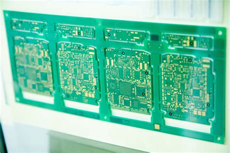
When designing High Density Interconnect (HDI) printed circuit boards (PCBs), several critical considerations must be taken into account to ensure optimal performance and reliability. HDI PCBs are characterized by their higher wiring density per unit area compared to traditional PCBs, achieved through the use of finer lines and spaces, smaller vias, and capture pads.
This increased density allows for more complex and compact designs, which are essential in modern electronic devices such as smartphones, tablets, and other compact gadgets. However, the intricate nature of HDI PCBs necessitates a meticulous approach to design.
One of the primary considerations in HDI PCB design is the selection of materials.
The materials used must support the fine features and high-density interconnections typical of HDI technology. This often involves choosing substrates with high glass transition temperatures (Tg) and low coefficients of thermal expansion (CTE) to ensure stability under thermal stress. Additionally, the dielectric constant and loss tangent of the materials should be carefully evaluated to maintain signal integrity, especially in high-frequency applications.
Another crucial aspect is the layer stack-up configuration. HDI PCBs often employ a combination of microvias, blind vias, and buried vias to achieve the desired interconnect density.
The stack-up must be designed to optimize the routing of signals while minimizing the number of layers to reduce cost and complexity. This involves strategic planning of via placement and the use of sequential lamination processes to build up the layers. The choice between different via technologies, such as laser-drilled microvias or mechanically drilled vias, can significantly impact the design and manufacturing process.
Signal integrity is a paramount concern in HDI PCB design due to the close proximity of traces and the potential for electromagnetic interference (EMI).
to mitigate these issues, designers must carefully consider trace width, spacing, and impedance control. Differential pair routing and the use of ground planes can help maintain signal quality and reduce crosstalk. Additionally, the implementation of proper shielding techniques and the strategic placement of decoupling capacitors are essential to ensure stable power delivery and minimize noise.
Thermal management is another critical consideration, as the compact nature of HDI PCBs can lead to increased heat generation.
Effective thermal management strategies, such as the use of thermal vias, heat sinks, and thermal interface materials, are necessary to dissipate heat and prevent overheating. The design must also account for the thermal conductivity of the materials used and the overall thermal profile of the device.
Furthermore, manufacturability and cost are important factors in HDI PCB design.
The complexity of HDI technology can lead to higher manufacturing costs, so it is essential to balance performance requirements with budget constraints. Collaborating closely with manufacturers during the design phase can help identify potential challenges and optimize the design for cost-effective production.
In conclusion, designing HDI PCBs requires a comprehensive understanding of material properties, layer stack-up configurations, signal integrity, thermal management, and manufacturability. By carefully considering these factors, designers can create high-performance, reliable, and cost-effective HDI PCBs that meet the demands of modern electronic applications. As technology continues to advance, the importance of meticulous HDI PCB design will only grow, underscoring the need for expertise and innovation in this field.
Manufacturing Challenges In High Density Interconnect (HDI) PCB Production
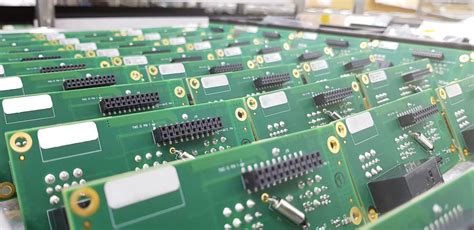
High Density Interconnect (HDI) PCBs have become a cornerstone in the advancement of modern electronics, offering enhanced performance and miniaturization capabilities. However, the production of HDI PCBs presents a unique set of manufacturing challenges that require careful consideration and innovative solutions. As the demand for smaller, more powerful electronic devices continues to grow, manufacturers are compelled to address these challenges to maintain efficiency and quality.
One of the primary challenges in HDI PCB production is the precision required in the fabrication process.
HDI PCBs are characterized by their fine lines and spaces, small vias, and high pad density, which necessitate advanced manufacturing techniques. The miniaturization of components means that even the slightest deviation in the manufacturing process can lead to significant defects.
Therefore, manufacturers must invest in state-of-the-art equipment and technologies, such as laser drilling and advanced photolithography, to achieve the necessary precision. These technologies, while effective, also introduce additional costs and complexity into the production process.
Moreover, the materials used in HDI PCBs pose another significant challenge.
The substrates and laminates must be carefully selected to withstand the thermal and mechanical stresses encountered during both manufacturing and operation. The choice of materials impacts not only the performance and reliability of the final product but also the manufacturability. For instance, materials with low dielectric constants are preferred for high-speed applications, yet they may be more difficult to process. Consequently, manufacturers must strike a balance between material properties and processability, often requiring extensive testing and validation.
In addition to material considerations, the aspect of layer alignment in HDI PCBs is critical.
As these PCBs often involve multiple layers, ensuring precise alignment is crucial to avoid short circuits and ensure signal integrity. Misalignment can lead to increased crosstalk and signal loss, which are detrimental to the performance of the device.
To mitigate this risk, manufacturers employ advanced registration systems and employ rigorous quality control measures throughout the production process.
However, these measures can increase production time and costs, presenting a further challenge in meeting market demands for rapid turnaround times.
Furthermore, the integration of microvias, a defining feature of HDI PCBs, introduces additional manufacturing complexities. Microvias are used to connect different layers within the PCB, and their small size requires precise drilling and plating techniques. The reliability of these microvias is paramount, as any failure can compromise the entire circuit. Manufacturers must therefore ensure that the plating process is meticulously controlled to prevent voids and ensure robust connections. This often involves the use of specialized plating chemistries and equipment, which can further complicate the manufacturing process.
Finally, the testing and inspection of HDI PCBs present their own set of challenges.
Given the complexity and density of these boards, traditional testing methods may not be sufficient to detect all potential defects. Advanced testing techniques, such as automated optical inspection (AOI) and X-ray inspection, are often employed to ensure the integrity of the final product. However, these methods can be time-consuming and costly, adding another layer of complexity to the production process.
In conclusion, while HDI PCBs offer significant advantages in terms of performance and miniaturization, their production is fraught with challenges that require careful management. From precision fabrication and material selection to layer alignment and microvia reliability, each aspect of the manufacturing process demands attention to detail and innovation. As technology continues to evolve, manufacturers must remain agile and adaptive, continually refining their processes to overcome these challenges and meet the ever-increasing demands of the electronics industry.
Future Trends In High Density Interconnect (HDI) PCB Technology
High Density Interconnect (HDI) PCB technology has been at the forefront of advancements in the electronics industry, offering a pathway to more compact, efficient, and powerful electronic devices. As we look to the future, several trends are poised to shape the evolution of HDI PCBs, driven by the relentless demand for miniaturization, enhanced performance, and cost-effectiveness.
One of the most significant trends is the increasing complexity of electronic devices, which necessitates more sophisticated HDI designs.
As devices become more multifunctional, the need for PCBs that can accommodate a higher number of components in a limited space becomes critical. This has led to the development of multi-layer HDI PCBs, which allow for more interconnections and components without increasing the overall size of the board. Consequently, manufacturers are investing in advanced fabrication techniques to produce these intricate designs with precision and reliability.
In addition to complexity, the demand for higher performance is driving innovations in HDI PCB materials.
Traditional materials are being replaced or supplemented with advanced composites that offer superior thermal management, electrical performance, and mechanical strength. These materials are essential for supporting the high-speed and high-frequency applications that are becoming increasingly common in sectors such as telecommunications, automotive, and consumer electronics. As a result, research and development efforts are focused on discovering and optimizing materials that can meet these stringent requirements while remaining cost-effective.
Moreover, the trend towards sustainability is influencing the future of HDI PCB technology.
As environmental concerns become more pressing, there is a growing emphasis on developing eco-friendly manufacturing processes and materials. This includes reducing the use of hazardous substances, improving energy efficiency during production, and enhancing the recyclability of PCBs. Manufacturers are exploring innovative approaches such as using biodegradable substrates and implementing closed-loop recycling systems to minimize waste and environmental impact.
Another key trend is the integration of advanced technologies such as artificial intelligence (AI) and the Internet of Things (IoT) into HDI PCBs.
These technologies require PCBs that can support complex data processing and connectivity functions. As a result, there is a push towards developing HDI PCBs with embedded components and sensors that can facilitate seamless communication and data exchange. This integration not only enhances the functionality of electronic devices but also opens up new possibilities for applications in smart homes, healthcare, and industrial automation.
Furthermore, the globalization of the electronics supply chain is influencing the future of HDI PCB technology.
As companies seek to optimize production costs and reduce time-to-market, there is a trend towards outsourcing PCB manufacturing to regions with advanced technological capabilities and competitive pricing. This has led to increased collaboration between manufacturers, designers, and suppliers across different countries, fostering innovation and the exchange of best practices.
In conclusion, the future of High Density Interconnect PCB technology is being shaped by a confluence of factors including the need for greater complexity, enhanced performance, sustainability, technological integration, and global collaboration.
As these trends continue to evolve, they will undoubtedly drive further advancements in HDI PCB technology, enabling the development of next-generation electronic devices that are more powerful, efficient, and environmentally friendly. The ongoing research and innovation in this field promise to unlock new possibilities and set new standards for the electronics industry in the years to come.