Hdi pcb material
Understanding The Benefits Of HDI PCB Material In Modern Electronics
High-Density Interconnect (HDI) printed circuit boards (PCBs) have become a cornerstone in the advancement of modern electronics, offering a multitude of benefits that cater to the ever-evolving demands of technology.
As electronic devices continue to shrink in size while increasing in functionality, the materials used in HDI PCBs play a crucial role in meeting these requirements.
Understanding the benefits of HDI PCB material is essential for appreciating their impact on the electronics industry.
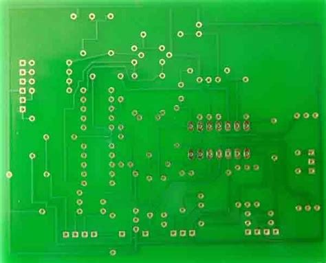
To begin with, HDI PCBs are characterized by their higher wiring density per unit area compared to traditional PCBs.
This is achieved through the use of finer lines and spaces, smaller vias, and capture pads, as well as higher connection pad density. The materials used in HDI PCBs are specifically chosen to support these features, providing enhanced electrical performance and reliability. For instance, the dielectric materials used in HDI PCBs often have lower dielectric constants and loss tangents, which contribute to improved signal integrity. This is particularly important in high-frequency applications where signal loss and interference can significantly impact performance.
Moreover, the materials used in HDI PCBs are designed to withstand the thermal and mechanical stresses associated with advanced manufacturing processes.
As electronic devices become more compact, the heat generated by densely packed components can pose a significant challenge. HDI PCB materials are engineered to offer superior thermal management, ensuring that heat is effectively dissipated and that the board remains stable under varying thermal conditions. This is achieved through the use of materials with high thermal conductivity and stability, which help maintain the integrity of the board and its components over time.
In addition to thermal management, the mechanical properties of HDI PCB materials are also of paramount importance.
The miniaturization of electronic devices necessitates the use of thinner and more flexible materials that can accommodate complex designs without compromising durability. HDI PCB materials are often reinforced with advanced composites that provide the necessary strength and flexibility, allowing for the creation of intricate multilayer designs that are both robust and reliable. This flexibility is particularly beneficial in applications where space is limited, such as in smartphones, tablets, and wearable devices.
Furthermore, the use of HDI PCB materials contributes to the overall reduction in size and weight of electronic devices.
By enabling the integration of more components into a smaller area, HDI PCBs allow for the development of compact and lightweight devices without sacrificing functionality. This is a significant advantage in industries such as aerospace and automotive, where reducing weight can lead to improved efficiency and performance.
In conclusion, the benefits of HDI PCB material in modern electronics are manifold, encompassing improved electrical performance, enhanced thermal and mechanical properties, and the facilitation of miniaturization. As technology continues to advance, the demand for smaller, more powerful electronic devices will only increase, further underscoring the importance of HDI PCB materials. By understanding these benefits, manufacturers and designers can better leverage the capabilities of HDI PCBs to create innovative solutions that meet the needs of today’s fast-paced technological landscape.
Key Differences Between HDI PCB Material And Traditional PCB Material
High-Density Interconnect (HDI) printed circuit boards (PCBs) have become increasingly prevalent in the electronics industry due to their ability to accommodate more complex and compact designs. Understanding the key differences between HDI PCB material and traditional PCB material is essential for engineers and designers who aim to optimize the performance and reliability of electronic devices. While both types of PCBs serve the fundamental purpose of connecting electronic components, the materials used in their construction significantly influence their capabilities and applications.
To begin with, one of the most notable differences between HDI and traditional PCB materials lies in their composition and structure.
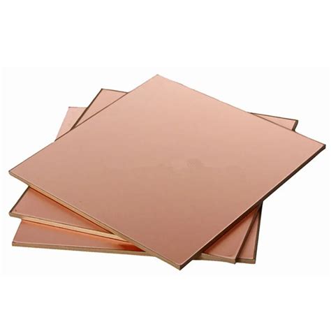
HDI PCBs typically utilize advanced materials such as modified epoxy resins, polyimide, or liquid crystal polymer (LCP), which offer superior thermal and mechanical properties. These materials are chosen for their ability to withstand the higher temperatures and mechanical stresses associated with dense circuitry. In contrast, traditional PCBs often use standard FR-4 material, a composite of woven fiberglass cloth with an epoxy resin binder, which, while cost-effective, may not provide the same level of performance in demanding applications.
Moreover, the choice of material in HDI PCBs allows for the incorporation of microvias, which are significantly smaller than the vias used in traditional PCBs.
Microvias enable the creation of finer lines and spaces, facilitating the design of more compact and efficient circuits. This is particularly advantageous in applications where space is at a premium, such as in smartphones, tablets, and other portable electronic devices. Traditional PCBs, on the other hand, are limited by the larger size of their vias, which can restrict the density of the circuitry and, consequently, the overall functionality of the device.
In addition to the structural differences, the electrical performance of HDI PCB materials often surpasses that of traditional materials.
The advanced materials used in HDI PCBs typically exhibit lower dielectric constants and dissipation factors, which contribute to reduced signal loss and improved signal integrity. This is crucial in high-frequency applications where maintaining signal quality is paramount. Traditional PCB materials, while adequate for many applications, may not offer the same level of electrical performance, particularly in high-speed or high-frequency environments.
Furthermore, the manufacturing processes for HDI and traditional PCBs differ significantly, largely due to the materials involved.
HDI PCBs require more sophisticated fabrication techniques, such as laser drilling for microvias and sequential lamination processes, to achieve the desired level of complexity and precision. These advanced processes, while more costly, enable the production of PCBs with multiple layers and intricate designs. In contrast, traditional PCBs are generally manufactured using more straightforward processes, which can be more economical but may not support the same level of complexity.
In conclusion, the key differences between HDI PCB material and traditional PCB material are rooted in their composition, structural capabilities, electrical performance, and manufacturing processes.
HDI PCBs, with their advanced materials and sophisticated fabrication techniques, offer significant advantages in terms of miniaturization, performance, and complexity, making them ideal for modern electronic applications. Traditional PCBs, while still widely used, may not provide the same level of performance in demanding environments. As technology continues to evolve, the choice between HDI and traditional PCB materials will increasingly depend on the specific requirements of the application and the desired balance between cost and performance.
How HDI PCB Material Enhances Performance In High-Density Applications
High-Density Interconnect (HDI) printed circuit boards (PCBs) have become a cornerstone in the advancement of modern electronics, particularly in applications where space and performance are critical. The choice of material in HDI PCBs plays a pivotal role in enhancing their performance, especially in high-density applications. As electronic devices continue to shrink in size while increasing in functionality, the demand for efficient and reliable HDI PCB materials has surged. Understanding how these materials contribute to performance improvements is essential for engineers and designers working in the field.
To begin with, HDI PCBs are characterized by their higher wiring density per unit area compared to traditional PCBs.
This is achieved through the use of finer lines and spaces, smaller vias, and capture pads, as well as higher connection pad density. The materials used in HDI PCBs must therefore support these features without compromising the board’s structural integrity or electrical performance. One of the primary materials used in HDI PCBs is a high-performance laminate, which provides the necessary mechanical support and thermal stability. These laminates are often reinforced with glass fibers and are designed to withstand the rigors of high-frequency applications.
Moreover, the dielectric material in HDI PCBs is crucial for maintaining signal integrity.
As the frequency of operation increases, the dielectric constant and loss tangent of the material become significant factors. Materials with low dielectric constants and low loss tangents are preferred as they minimize signal loss and crosstalk, which are critical in high-speed applications. This ensures that the signals transmitted through the PCB remain clear and undistorted, thereby enhancing the overall performance of the device.
In addition to dielectric properties, the thermal management capabilities of HDI PCB materials are of paramount importance.
As electronic components become more densely packed, the heat generated within the PCB can lead to performance degradation or even failure. Therefore, materials with high thermal conductivity are employed to efficiently dissipate heat away from critical components. This not only prolongs the lifespan of the device but also ensures consistent performance under varying operating conditions.
Furthermore, the choice of copper foil in HDI PCBs is another factor that influences performance.
Thinner copper foils are often used to achieve finer traces, which are essential for high-density applications. However, these foils must also exhibit excellent adhesion to the substrate to prevent delamination and ensure reliable electrical connections. Advanced surface treatments and bonding techniques are employed to enhance the adhesion properties of copper foils, thereby improving the durability and reliability of the HDI PCB.
In conclusion, the materials used in HDI PCBs are integral to their ability to perform in high-density applications. By carefully selecting materials with the appropriate mechanical, electrical, and thermal properties, engineers can design PCBs that meet the demanding requirements of modern electronic devices. As technology continues to evolve, the development of new materials and fabrication techniques will further enhance the capabilities of HDI PCBs, enabling even more compact and powerful electronic solutions. The ongoing research and innovation in this field underscore the importance of material science in the advancement of electronic technology, ensuring that HDI PCBs remain at the forefront of high-performance applications.
Innovations In HDI PCB Material: What To Expect In The Future
High-Density Interconnect (HDI) printed circuit boards (PCBs) have become a cornerstone in the advancement of modern electronics, offering enhanced performance and miniaturization capabilities. As the demand for more compact and efficient electronic devices continues to rise, innovations in HDI PCB materials are crucial to meeting these evolving needs. The future of HDI PCB materials is poised to bring about significant changes, driven by technological advancements and the pursuit of sustainability.
To begin with, one of the most promising areas of innovation in HDI PCB materials is the development of advanced substrates.
Traditional materials such as FR-4 have served the industry well, but they are reaching their limits in terms of thermal management and signal integrity. Consequently, researchers are exploring alternative materials like liquid crystal polymer (LCP) and polytetrafluoroethylene (PTFE), which offer superior dielectric properties and thermal stability. These materials are expected to play a pivotal role in the next generation of HDI PCBs, enabling higher frequency applications and improved performance.
Moreover, the integration of nanotechnology into HDI PCB materials is another exciting frontier.
By incorporating nanoparticles into the substrate, manufacturers can enhance the mechanical and electrical properties of the boards. For instance, the use of carbon nanotubes can significantly improve thermal conductivity, which is essential for managing the heat generated by densely packed components. This innovation not only extends the lifespan of electronic devices but also supports the trend towards more powerful and compact gadgets.
In addition to these material advancements, the industry is also focusing on sustainability.
As environmental concerns become increasingly prominent, there is a growing emphasis on developing eco-friendly HDI PCB materials. This includes the use of biodegradable substrates and the reduction of hazardous substances in the manufacturing process. By prioritizing sustainability, the industry aims to minimize its environmental footprint while still delivering high-performance products.
Furthermore, the advent of flexible HDI PCBs is set to revolutionize the design and application of electronic devices.
Flexible materials such as polyimide and polyethylene naphthalate (PEN) allow for the creation of bendable and foldable circuits, opening up new possibilities in wearable technology and other innovative applications. As these materials continue to evolve, they will enable the development of electronics that are not only more versatile but also more integrated into everyday life.
In parallel with these material innovations, advancements in manufacturing techniques are also expected to drive the future of HDI PCBs.
Techniques such as laser direct imaging (LDI) and additive manufacturing are becoming more prevalent, allowing for greater precision and efficiency in the production of complex circuit designs. These methods not only reduce production costs but also facilitate the rapid prototyping and customization of HDI PCBs, catering to the diverse needs of various industries.
In conclusion, the future of HDI PCB materials is set to be shaped by a combination of advanced substrates, nanotechnology, sustainability efforts, flexible materials, and innovative manufacturing techniques. As these developments continue to unfold, they will undoubtedly lead to more powerful, efficient, and environmentally friendly electronic devices. The ongoing research and investment in this field underscore the importance of HDI PCBs in the ever-evolving landscape of technology, promising a future where electronic devices are more capable and adaptable than ever before.