Hdi pcb factory
Innovations in HDI PCB Manufacturing: What Sets Modern Factories Apart
In recent years, the landscape of high-density interconnect (HDI) printed circuit board (PCB) manufacturing has undergone significant transformation, driven by technological advancements and the increasing demand for more compact and efficient electronic devices. Modern HDI PCB factories have embraced a range of innovative practices and technologies that set them apart from traditional manufacturing facilities. These innovations not only enhance the quality and performance of the PCBs but also improve the efficiency and sustainability of the manufacturing process.
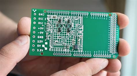
One of the most notable advancements in HDI PCB manufacturing is the adoption of laser drilling technology.
Unlike conventional mechanical drilling, laser drilling allows for the creation of microvias with exceptional precision and accuracy. This technology enables manufacturers to produce PCBs with higher layer counts and finer lines, which are essential for accommodating the complex circuitry required by modern electronic devices. Moreover, laser drilling reduces the risk of damage to the substrate, thereby increasing the overall reliability of the finished product.
In addition to laser drilling, the use of advanced materials has also contributed to the evolution of HDI PCB manufacturing.
Modern factories are increasingly utilizing high-performance laminates and substrates that offer superior thermal and electrical properties. These materials not only support the miniaturization of electronic components but also enhance the durability and longevity of the PCBs. Furthermore, the integration of these advanced materials into the manufacturing process has facilitated the development of flexible and rigid-flex PCBs, which are crucial for applications in industries such as aerospace, automotive, and consumer electronics.
Another key innovation in HDI PCB manufacturing is the implementation of automated production systems.
Automation has revolutionized the way PCBs are produced, allowing for greater precision, consistency, and speed. Automated systems can handle complex tasks such as solder paste application, component placement, and inspection with minimal human intervention. This not only reduces the likelihood of errors but also increases production throughput, enabling factories to meet the growing demand for HDI PCBs more efficiently. Additionally, automation contributes to cost savings by minimizing labor expenses and reducing material waste.
Sustainability has also become a focal point in modern HDI PCB manufacturing.
Factories are increasingly adopting eco-friendly practices to minimize their environmental impact. For instance, many facilities have implemented closed-loop water systems to reduce water consumption and prevent pollution. Additionally, the use of lead-free solder and other environmentally friendly materials has become standard practice, aligning with global regulations and consumer expectations for sustainable products. These efforts not only benefit the environment but also enhance the reputation of manufacturers as responsible and forward-thinking entities.
Furthermore, the integration of advanced quality control measures has set modern HDI PCB factories apart.
The use of sophisticated inspection technologies, such as automated optical inspection (AOI) and X-ray inspection, ensures that each PCB meets stringent quality standards. These technologies can detect even the smallest defects, allowing manufacturers to address issues before the products reach the market. This commitment to quality not only reduces the risk of product failures but also strengthens customer trust and satisfaction.
In conclusion, the innovations in HDI PCB manufacturing have significantly elevated the capabilities and efficiency of modern factories.
Through the adoption of laser drilling, advanced materials, automation, sustainability practices, and rigorous quality control, these facilities are well-equipped to meet the demands of an ever-evolving electronics industry. As technology continues to advance, it is likely that HDI PCB manufacturing will continue to evolve, further enhancing the performance and reliability of electronic devices worldwide.
The Role of Automation in HDI PCB Factories: Enhancing Efficiency and Precision
In the rapidly evolving landscape of electronics manufacturing, High-Density Interconnect (HDI) printed circuit boards (PCBs) have emerged as a cornerstone of modern technology. As the demand for smaller, more powerful electronic devices continues to grow, the role of automation in HDI PCB factories has become increasingly significant. Automation not only enhances efficiency but also ensures precision, which is crucial in meeting the stringent requirements of today’s electronic components.
To begin with, automation in HDI PCB factories streamlines the production process by minimizing human intervention.
This reduction in manual labor not only accelerates production but also significantly reduces the likelihood of human error. Automated systems are capable of performing repetitive tasks with consistent accuracy, which is essential in the intricate process of HDI PCB manufacturing. For instance, automated drilling machines can precisely create microvias, which are tiny holes that connect different layers of a PCB. The precision required in this task is beyond the capability of manual operations, highlighting the indispensable role of automation.
Moreover, automation facilitates enhanced quality control in HDI PCB production.
Automated inspection systems, equipped with advanced imaging technologies, can detect defects at a microscopic level. These systems ensure that each PCB meets the high standards required for modern electronic devices. By identifying defects early in the production process, manufacturers can reduce waste and improve overall product quality. This level of precision is particularly important in industries such as aerospace and medical devices, where the reliability of electronic components is paramount.
In addition to improving quality, automation also contributes to increased production efficiency.
Automated assembly lines can operate continuously, significantly boosting output compared to manual processes. This capability is particularly beneficial in meeting the high-volume demands of consumer electronics. Furthermore, automation allows for greater flexibility in production. Advanced software systems enable quick reconfiguration of manufacturing processes, allowing factories to adapt swiftly to changes in product design or demand. This adaptability is crucial in the fast-paced world of electronics, where product lifecycles are becoming increasingly short.
Transitioning to the economic implications, the integration of automation in HDI PCB factories can lead to substantial cost savings.
While the initial investment in automated systems can be significant, the long-term benefits often outweigh these costs. Reduced labor expenses, lower defect rates, and increased production speeds contribute to a more cost-effective manufacturing process. Additionally, automation can help mitigate the impact of labor shortages, a growing concern in many regions. By relying on automated systems, factories can maintain high levels of productivity even in the face of workforce challenges.
Finally, it is important to consider the role of automation in fostering innovation within the HDI PCB industry.
As automated systems become more sophisticated, they open up new possibilities for design and functionality. For example, advanced robotics and machine learning algorithms can optimize PCB layouts for better performance and efficiency. This capability not only enhances existing products but also paves the way for the development of new technologies.
In conclusion, the role of automation in HDI PCB factories is multifaceted, encompassing improvements in efficiency, precision, quality control, and cost-effectiveness. As technology continues to advance, the integration of automation in PCB manufacturing will undoubtedly play a crucial role in shaping the future of electronics. By embracing these innovations, HDI PCB factories can meet the demands of an ever-evolving market while maintaining the highest standards of quality and reliability.
Sustainability Practices in HDI PCB Factories: Reducing Environmental Impact
In recent years, the electronics industry has witnessed a significant shift towards more sustainable practices, particularly in the manufacturing of high-density interconnect (HDI) printed circuit boards (PCBs). As the demand for smaller, more efficient electronic devices grows, so does the need for HDI PCBs, which offer enhanced performance and miniaturization capabilities. However, the production of these advanced circuit boards can have substantial environmental impacts if not managed responsibly. Consequently, HDI PCB factories are increasingly adopting sustainability practices to mitigate their ecological footprint and promote environmental stewardship.
One of the primary areas of focus for HDI PCB factories is the reduction of hazardous waste.
The manufacturing process involves the use of various chemicals, including etchants and solvents, which can pose significant environmental risks if not handled properly. To address this, many factories are implementing closed-loop systems that recycle and reuse these chemicals, thereby minimizing waste generation. Additionally, advancements in chemical formulations have led to the development of less toxic alternatives, further reducing the potential for environmental harm.
Energy consumption is another critical aspect of sustainability in HDI PCB production.
The intricate processes involved in manufacturing these boards, such as laser drilling and plating, require substantial energy inputs. To combat this, factories are investing in energy-efficient technologies and equipment. For instance, the adoption of LED lighting, high-efficiency motors, and advanced heating systems can significantly reduce energy usage. Moreover, some facilities are integrating renewable energy sources, such as solar or wind power, into their operations, thereby decreasing their reliance on fossil fuels and lowering their carbon footprint.
Water conservation is also a key component of sustainable practices in HDI PCB factories.
The production process typically involves significant water usage, particularly in cleaning and rinsing stages. To address this, many factories are implementing water recycling systems that treat and reuse water within the facility.
This not only conserves a vital resource but also reduces the discharge of potentially contaminated water into the environment. Furthermore, by optimizing water usage and employing closed-loop systems, factories can achieve substantial reductions in water consumption.
In addition to these measures, HDI PCB factories are increasingly focusing on sustainable sourcing of raw materials.
The use of conflict-free minerals and materials from certified sustainable sources is becoming a standard practice. This not only ensures compliance with international regulations but also supports ethical supply chains and reduces the environmental impact associated with raw material extraction and processing.
Employee engagement and training also play a crucial role in the successful implementation of sustainability practices.
By fostering a culture of environmental awareness and responsibility, factories can empower their workforce to contribute to sustainability goals. Regular training sessions and workshops can equip employees with the knowledge and skills needed to identify and implement eco-friendly practices in their daily tasks.
In conclusion, the adoption of sustainability practices in HDI PCB factories is essential for reducing their environmental impact and promoting a more sustainable electronics industry. Through the implementation of waste reduction strategies, energy-efficient technologies, water conservation measures, sustainable sourcing, and employee engagement, these factories are making significant strides towards minimizing their ecological footprint. As the demand for HDI PCBs continues to grow, it is imperative that the industry remains committed to these practices, ensuring a balance between technological advancement and environmental responsibility.
Quality Control Measures in HDI PCB Production: Ensuring Reliability and Performance
In the realm of electronics manufacturing, the production of High-Density Interconnect (HDI) printed circuit boards (PCBs) stands as a critical process, demanding meticulous attention to quality control measures. These advanced PCBs, characterized by their compact design and high performance, are integral to modern electronic devices, from smartphones to aerospace technology. Ensuring the reliability and performance of HDI PCBs necessitates a comprehensive approach to quality control, encompassing every stage of production.
To begin with, the selection of raw materials is a foundational aspect of quality control in HDI PCB production.
The materials used must meet stringent specifications to ensure they can withstand the demands of high-density applications. This involves rigorous testing of substrates, copper foils, and other components to verify their properties, such as thermal stability and electrical conductivity. By ensuring that only high-quality materials are used, manufacturers can prevent defects and enhance the overall performance of the final product.
As the production process progresses, precision in manufacturing becomes paramount.
Advanced fabrication techniques, such as laser drilling and microvia technology, are employed to achieve the intricate designs required for HDI PCBs. These techniques demand exacting precision, as even minor deviations can lead to significant performance issues. Therefore, continuous monitoring and calibration of equipment are essential to maintain the accuracy of these processes. Automated inspection systems, utilizing technologies like optical and X-ray inspection, play a crucial role in identifying defects at this stage, allowing for immediate corrective actions.
Furthermore, the multilayer nature of HDI PCBs introduces additional complexity to the quality control process.
Each layer must be perfectly aligned and bonded to ensure optimal electrical performance. This requires precise control over the lamination process, where temperature, pressure, and time must be meticulously regulated. Any misalignment or delamination can compromise the integrity of the entire board, leading to potential failures in the field. Consequently, thorough inspections are conducted after each lamination cycle to detect and rectify any issues before proceeding to the next stage.
In addition to these manufacturing controls, electrical testing is a critical component of quality assurance in HDI PCB production.
This involves subjecting the boards to a series of tests to verify their electrical properties and functionality. Techniques such as flying probe testing and in-circuit testing are employed to ensure that each circuit path is correctly formed and that there are no short circuits or open connections. These tests are vital in confirming that the boards will perform reliably under real-world conditions.
Moreover, environmental testing is conducted to assess the durability of HDI PCBs under various conditions.
This includes thermal cycling, humidity exposure, and vibration testing, which simulate the stresses the boards will encounter during their operational life. By subjecting the boards to these rigorous tests, manufacturers can identify potential weaknesses and make necessary improvements to enhance their resilience.
In conclusion, the production of HDI PCBs is a complex process that demands a robust quality control framework to ensure reliability and performance. From the careful selection of materials to precision manufacturing and comprehensive testing, each step is critical in delivering high-quality PCBs that meet the exacting standards of modern electronic applications. Through these meticulous quality control measures, manufacturers can provide assurance to their clients that their products will perform as expected, even in the most demanding environments.