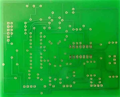
3+n+3 hdi pcb
Understanding the Advantages of 3+n+3 HDI PCB in Modern Electronics
In the rapidly evolving landscape of modern electronics, the demand for more compact, efficient, and high-performance devices has led to significant advancements in printed circuit board (PCB) technology.
Among these innovations, the 3+n+3 High-Density Interconnect (HDI) PCB stands out as a pivotal development, offering numerous advantages that cater to the needs of contemporary electronic applications. Understanding the benefits of 3+n+3 HDI PCBs is essential for engineers and designers aiming to optimize their products for the competitive market.
To begin with, the 3+n+3 HDI PCB is characterized by its multilayer structure, which typically consists of three sequential build-up layers on both sides of a core layer.
This configuration allows for a higher density of interconnections compared to traditional PCBs, thereby enabling more complex circuitry within a smaller footprint. As a result, devices can be made more compact without compromising on functionality, a crucial factor in the design of modern electronics such as smartphones, tablets, and wearable technology.
Moreover, the enhanced interconnect density of 3+n+3 HDI PCBs facilitates improved electrical performance.
The shorter and more direct routing paths reduce signal loss and electromagnetic interference, which are common challenges in high-speed digital circuits. Consequently, this leads to faster signal transmission and improved overall performance of the electronic device. Additionally, the use of microvias in HDI PCBs, which are smaller than conventional vias, further contributes to the reduction of parasitic capacitance and inductance, enhancing signal integrity.
Another significant advantage of 3+n+3 HDI PCBs is their contribution to thermal management.
As electronic devices become more powerful, they generate more heat, which can adversely affect performance and reliability. The multilayer structure of HDI PCBs allows for better heat dissipation, as the heat can be spread across multiple layers and away from critical components. This is particularly beneficial in applications where maintaining optimal operating temperatures is crucial, such as in automotive electronics and high-performance computing.
In addition to performance benefits, 3+n+3 HDI PCBs offer greater design flexibility.
The ability to incorporate more components and interconnections within a limited space provides designers with the freedom to innovate and create more sophisticated electronic products. This flexibility is especially valuable in industries where miniaturization and functionality are key competitive factors, such as in consumer electronics and medical devices.
Furthermore, the adoption of 3+n+3 HDI PCBs can lead to cost savings in the long run.
Although the initial manufacturing costs may be higher due to the complexity of the design and fabrication processes, the reduction in size and weight of the final product can result in lower material and shipping costs. Additionally, the improved reliability and performance of devices using HDI technology can lead to fewer failures and reduced maintenance costs over time.
In conclusion, the 3+n+3 HDI PCB represents a significant advancement in PCB technology, offering numerous advantages that align with the demands of modern electronic applications. Its ability to support higher interconnect density, improve electrical performance, enhance thermal management, and provide design flexibility makes it an invaluable asset in the development of cutting-edge electronic devices. As the electronics industry continues to push the boundaries of innovation, the role of 3+n+3 HDI PCBs is likely to become increasingly prominent, driving further advancements and enabling the creation of more sophisticated and efficient products.
Design Challenges and Solutions for 3+n+3 HDI PCB
The design of 3+n+3 High-Density Interconnect (HDI) printed circuit boards (PCBs) presents a unique set of challenges and solutions that are critical for modern electronic applications. As electronic devices continue to shrink in size while increasing in functionality, the demand for more complex and compact PCBs has grown. The 3+n+3 HDI PCB, characterized by its three layers of microvias on both the top and bottom, with n number of buried layers in between, offers a sophisticated solution to meet these demands. However, designing such intricate PCBs requires careful consideration of several factors to ensure optimal performance and reliability.
One of the primary challenges in designing 3+n+3 HDI PCBs is managing the increased density of interconnections.
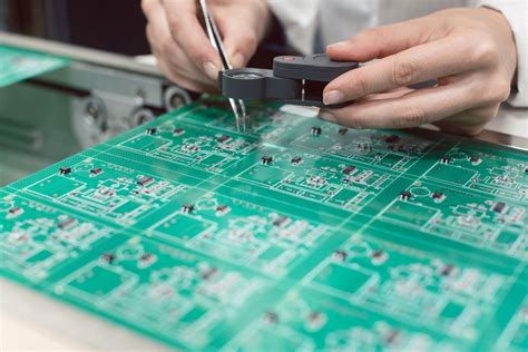
As the number of layers and vias increases, so does the complexity of routing signals without causing interference or crosstalk. To address this, designers must employ advanced routing techniques and tools that can efficiently handle the intricate web of connections. Utilizing computer-aided design (CAD) software with robust simulation capabilities allows designers to visualize and optimize the signal paths, ensuring that they meet the necessary electrical performance criteria.
Moreover, thermal management becomes a significant concern in 3+n+3 HDI PCBs due to the compact nature of the design.
The close proximity of components and interconnections can lead to hotspots, which may affect the board’s performance and longevity. To mitigate this, designers often incorporate thermal vias and strategically place heat-dissipating materials within the PCB stack-up. Additionally, selecting materials with high thermal conductivity for the PCB substrate can help in effectively managing heat dissipation.
Another challenge is the mechanical reliability of the PCB, particularly concerning the microvias.
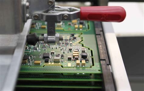
The repeated thermal cycling that PCBs undergo during operation can lead to fatigue and failure of these tiny interconnections. To enhance reliability, designers may opt for staggered or stacked microvia configurations, depending on the specific application requirements. Furthermore, employing advanced fabrication techniques, such as laser drilling and sequential lamination, can improve the precision and durability of the microvias.
Signal integrity is also a critical consideration in the design of 3+n+3 HDI PCBs.
The high-speed signals that these boards often carry are susceptible to degradation due to impedance mismatches and electromagnetic interference. To combat this, designers must carefully control the impedance of the traces and use differential signaling where possible. Additionally, incorporating ground planes and shielding can help minimize electromagnetic interference, ensuring that the signals maintain their integrity throughout the board.
Finally, cost considerations cannot be overlooked in the design process.
While 3+n+3 HDI PCBs offer significant advantages in terms of performance and miniaturization, they are inherently more expensive to produce than traditional PCBs. Designers must balance the need for advanced features with budget constraints, often requiring trade-offs in material selection and manufacturing processes. Collaborating closely with manufacturers during the design phase can help identify cost-effective solutions without compromising on quality.
In conclusion, the design of 3+n+3 HDI PCBs involves navigating a complex landscape of challenges, from managing interconnection density and thermal performance to ensuring mechanical reliability and signal integrity. By leveraging advanced design tools and techniques, and maintaining a close partnership with manufacturers, designers can overcome these challenges and deliver high-performance PCBs that meet the demands of modern electronic applications.
Applications of 3+n+3 HDI PCB in High-Tech Industries
The advent of 3+n+3 High-Density Interconnect (HDI) printed circuit boards (PCBs) has significantly transformed the landscape of high-tech industries, offering unprecedented opportunities for innovation and efficiency. These advanced PCBs, characterized by their multilayer structure and microvia technology, are increasingly being adopted across various sectors due to their ability to support complex circuitry in compact designs. As industries continue to push the boundaries of technology, the applications of 3+n+3 HDI PCBs are becoming more diverse and integral to the development of cutting-edge solutions.
One of the primary industries benefiting from 3+n+3 HDI PCBs is the consumer electronics sector.
With the relentless demand for smaller, more powerful devices, manufacturers are turning to these PCBs to meet the challenge. Smartphones, tablets, and wearable technology are prime examples where 3+n+3 HDI PCBs are utilized to accommodate intricate circuitry within limited space, thereby enhancing functionality without compromising on size. The ability to integrate more components into a smaller area not only improves performance but also contributes to the sleek, compact designs that consumers desire.
In addition to consumer electronics, the automotive industry is also leveraging the advantages of 3+n+3 HDI PCBs.
As vehicles become increasingly sophisticated with the integration of advanced driver-assistance systems (ADAS), infotainment systems, and electric powertrains, the need for reliable and efficient electronic components is paramount. 3+n+3 HDI PCBs provide the necessary support for these complex systems, ensuring seamless communication between various electronic modules. This capability is crucial for the development of autonomous vehicles, where precision and reliability are non-negotiable.
Moreover, the telecommunications industry is experiencing a paradigm shift with the deployment of 5G technology, which demands high-speed data transmission and low latency. 3+n+3 HDI PCBs are instrumental in meeting these requirements, as they facilitate the design of high-frequency circuits with minimal signal loss. This is particularly important in the development of base stations and network infrastructure, where performance and efficiency are critical. By enabling faster and more reliable communication, these PCBs are playing a pivotal role in the global rollout of 5G networks.
Furthermore, the medical field is witnessing a surge in the use of 3+n+3 HDI PCBs, particularly in the design of medical devices that require precision and reliability.
From diagnostic equipment to implantable devices, the ability to incorporate complex circuitry in a compact form factor is essential. These PCBs support the miniaturization of medical devices, allowing for less invasive procedures and improved patient outcomes. As medical technology continues to evolve, the demand for advanced PCBs is expected to grow, further cementing their role in the industry.
In conclusion, the applications of 3+n+3 HDI PCBs in high-tech industries are vast and varied, driven by the need for compact, efficient, and reliable electronic solutions. As technology continues to advance, these PCBs will undoubtedly play a crucial role in shaping the future of various sectors, from consumer electronics and automotive to telecommunications and healthcare. By enabling the development of innovative products and systems, 3+n+3 HDI PCBs are not only meeting current demands but also paving the way for future technological breakthroughs.
Future Trends in 3+n+3 HDI PCB Technology
The evolution of printed circuit board (PCB) technology has been marked by continuous innovation, with High-Density Interconnect (HDI) PCBs standing at the forefront of this advancement.
Among the various configurations, the 3+n+3 HDI PCB design is gaining significant attention due to its ability to support complex electronic applications. As we look to the future, several trends are poised to shape the development and utilization of 3+n+3 HDI PCBs, driven by the increasing demand for miniaturization, enhanced performance, and cost efficiency.
To begin with, the trend towards miniaturization in electronic devices is a primary driver for the adoption of 3+n+3 HDI PCBs.
These PCBs are characterized by their multiple layers, which allow for a higher density of components and interconnections within a smaller footprint. This is particularly advantageous in industries such as consumer electronics, automotive, and telecommunications, where space is at a premium. As devices continue to shrink in size while increasing in functionality, the ability of 3+n+3 HDI PCBs to accommodate more components without compromising performance becomes increasingly valuable.
Moreover, the demand for enhanced performance in electronic devices is pushing the boundaries of what 3+n+3 HDI PCBs can achieve.
These PCBs offer improved electrical performance due to their shorter signal paths and reduced parasitic effects, which are critical for high-speed and high-frequency applications. As technology advances, the need for faster data processing and transmission speeds will further drive the development of 3+n+3 HDI PCBs with even more sophisticated designs and materials. This will likely include the integration of advanced materials such as low-loss dielectrics and high-speed laminates, which can support the rigorous demands of next-generation applications.
In addition to performance improvements, cost efficiency remains a significant consideration in the future of 3+n+3 HDI PCB technology.
While the initial manufacturing costs of these complex PCBs can be higher than traditional designs, advancements in fabrication techniques are expected to reduce costs over time. Innovations such as laser drilling, advanced plating processes, and automated assembly are contributing to more efficient production methods. As these technologies mature, they will likely lead to a decrease in production costs, making 3+n+3 HDI PCBs more accessible to a broader range of applications and industries.
Furthermore, the rise of the Internet of Things (IoT) and wearable technology is expected to further propel the demand for 3+n+3 HDI PCBs.
These applications require compact, reliable, and high-performance PCBs to function effectively. The ability of 3+n+3 HDI PCBs to provide robust interconnect solutions in a compact form factor makes them ideal for IoT devices and wearables, which are becoming increasingly prevalent in both consumer and industrial markets.
In conclusion, the future trends in 3+n+3 HDI PCB technology are shaped by the ongoing pursuit of miniaturization, enhanced performance, and cost efficiency. As electronic devices continue to evolve, the role of 3+n+3 HDI PCBs will become even more critical in meeting the demands of modern applications. With advancements in materials, fabrication techniques, and design methodologies, these PCBs are well-positioned to support the next wave of technological innovation, ensuring their relevance and importance in the ever-changing landscape of electronics.