Apa itu printed circuit board
Introduction To Printed Circuit Boards: Understanding The Basics
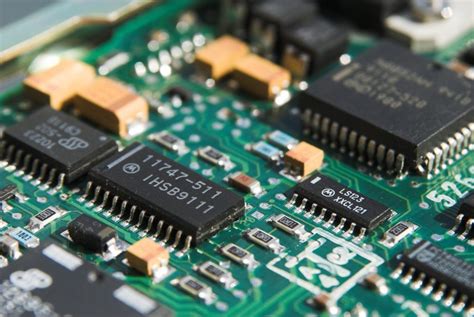
Printed Circuit Boards (PCBs) are fundamental components in modern electronic devices, serving as the backbone that supports and connects various electronic components. Understanding the basics of PCBs is essential for anyone interested in electronics, as these boards are integral to the functionality of a wide range of devices, from simple gadgets to complex machinery.
At their core, PCBs are designed to mechanically support and electrically connect electronic components using conductive pathways, tracks, or signal traces etched from copper sheets laminated onto a non-conductive substrate.
The development of PCBs marked a significant advancement in the field of electronics, allowing for more compact and reliable designs compared to earlier methods of circuit construction, such as point-to-point wiring.
This innovation not only streamlined the manufacturing process but also enhanced the performance and durability of electronic devices. The substrate, typically made from materials like fiberglass, epoxy, or other composite materials, provides the necessary insulation and structural support. Meanwhile, the copper traces form the electrical connections between components, ensuring efficient signal transmission.
Transitioning from the basic structure, it is important to consider the various types of PCBs available, each suited to different applications.
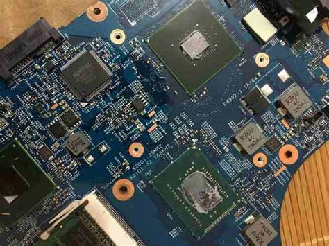
Single-sided PCBs, the simplest form, have components mounted on one side of the board and are commonly used in low-cost, low-density applications. Double-sided PCBs, on the other hand, have components on both sides, allowing for more complex circuits and increased component density. For even more intricate designs, multi-layer PCBs are employed, consisting of multiple layers of substrate and circuitry stacked together. These are essential in high-performance applications such as computers and telecommunications equipment, where space is at a premium and complex routing is required.
Moreover, the design and manufacturing process of PCBs is a meticulous task that involves several stages, from schematic design to layout and fabrication.
The design phase begins with creating a schematic diagram that outlines the electrical connections and components. This is followed by the layout process, where the physical arrangement of components and routing of traces are determined. Advanced software tools are often used to optimize this process, ensuring that the final design meets all electrical and mechanical requirements.
Once the design is finalized, the fabrication process begins, involving the etching of copper layers, drilling of holes for component leads, and application of solder masks and silkscreens. Quality control is a critical aspect of this process, as any defects can lead to malfunctioning circuits. Therefore, rigorous testing is conducted to ensure that the PCBs meet the required standards and specifications.
In conclusion, Printed Circuit Boards are indispensable in the realm of electronics, providing the necessary infrastructure for the operation of countless devices. Their evolution from simple single-sided boards to complex multi-layer configurations reflects the advancements in technology and the growing demands of modern applications. Understanding the basics of PCBs, from their structure and types to the design and manufacturing processes, is crucial for anyone involved in electronics, whether as a hobbyist or a professional. As technology continues to advance, the role of PCBs will undoubtedly expand, further cementing their importance in the ever-evolving landscape of electronic innovation.
The Evolution Of Printed Circuit Boards: From Inception To Modern Day
Printed circuit boards (PCBs) have become an integral component of modern electronic devices, serving as the backbone that supports and connects various electronic components. The evolution of PCBs from their inception to the present day is a fascinating journey that highlights the rapid advancements in technology and manufacturing processes. Initially, electronic circuits were constructed using point-to-point wiring, a labor-intensive and error-prone method. This approach involved manually connecting each component with wires, which often resulted in unreliable connections and limited the complexity of the circuits that could be built.
The need for a more efficient and reliable method of constructing electronic circuits led to the development of the printed circuit board.
The concept of a PCB was first introduced in the early 20th century, with the invention of the printed wire technique by Albert Hanson in 1903. However, it was not until the 1940s that PCBs began to gain widespread use, particularly during World War II, when they were employed in military radios and other equipment. This period marked the beginning of the transition from point-to-point wiring to the more efficient and reliable PCB technology.
As the demand for more compact and complex electronic devices grew, so did the need for advancements in PCB technology.
The introduction of the through-hole technology in the 1950s allowed for components to be mounted on the board by inserting their leads into pre-drilled holes and soldering them in place. This development significantly improved the durability and reliability of electronic circuits, paving the way for more sophisticated designs. However, the size and weight of these early PCBs were still a limiting factor in the miniaturization of electronic devices.
The next major leap in PCB evolution came with the advent of surface mount technology (SMT) in the 1980s.
SMT allowed components to be mounted directly onto the surface of the board, eliminating the need for through-holes and enabling the production of smaller, lighter, and more densely packed PCBs. This innovation was crucial in the development of modern electronics, as it facilitated the creation of compact devices such as smartphones, laptops, and wearable technology. Moreover, SMT improved the efficiency of the manufacturing process, reducing costs and increasing production speed.
In recent years, the evolution of PCBs has continued to accelerate, driven by the ever-increasing demand for more powerful and efficient electronic devices.
Advances in materials science have led to the development of flexible PCBs, which can be bent and shaped to fit into unconventional spaces, further expanding the possibilities for electronic design. Additionally, the integration of advanced technologies such as embedded components and multi-layer PCBs has enabled the creation of highly complex circuits with enhanced performance and functionality.
As we look to the future, the evolution of printed circuit boards is likely to be shaped by emerging technologies such as the Internet of Things (IoT), artificial intelligence, and 5G connectivity.
These advancements will undoubtedly drive further innovation in PCB design and manufacturing, enabling the development of even more sophisticated and efficient electronic devices. In conclusion, the journey of printed circuit boards from their inception to the modern day is a testament to the relentless pursuit of technological progress, and their continued evolution will undoubtedly play a crucial role in shaping the future of electronics.
Key Components And Materials Used In Printed Circuit Boards
Printed circuit boards (PCBs) are the backbone of modern electronic devices, serving as the foundation upon which electronic components are mounted and interconnected. Understanding the key components and materials used in PCBs is essential for appreciating their role in the functionality and reliability of electronic systems.
At the heart of a PCB is the substrate, typically made from a material known as FR-4, which is a composite of woven fiberglass cloth with an epoxy resin binder that is flame resistant.
This material provides the necessary mechanical support and electrical insulation for the board. The choice of substrate material is crucial, as it affects the board’s thermal and electrical properties, as well as its overall durability.
On top of the substrate, a thin layer of copper foil is laminated to one or both sides of the board.
This copper layer is etched to form the circuit patterns that connect different components. The thickness of the copper layer can vary depending on the board’s intended application, with thicker layers used for high-power applications to accommodate higher current loads. The etching process is a critical step in PCB manufacturing, as it defines the pathways for electrical signals to travel across the board. Once the copper patterns are established, a solder mask is applied over the copper traces. This protective layer, usually green but available in various colors, prevents solder from bridging between conductors and protects the copper from environmental damage and oxidation.
In addition to the substrate, copper, and solder mask, PCBs also incorporate a silkscreen layer.
This layer is used to print text and symbols on the board, providing valuable information such as component labels, part numbers, and company logos. The silkscreen is typically applied in white ink, although other colors can be used for aesthetic or functional purposes. The clarity and accuracy of the silkscreen are important for assembly and maintenance, as they guide technicians in placing and identifying components.
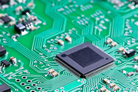
The components mounted on a PCB are connected through a combination of through-hole and surface-mount technologies.
Through-hole components have leads that are inserted into holes drilled through the board and soldered to pads on the opposite side. This method provides strong mechanical bonds and is often used for components that require high reliability or mechanical strength. In contrast, surface-mount technology (SMT) involves placing components directly onto the surface of the board, where they are soldered to pads without the need for drilled holes. SMT allows for higher component density and is favored in modern electronics for its efficiency and space-saving advantages.
The choice of materials and components in PCB design is influenced by several factors, including the intended application, environmental conditions, and cost considerations.
For instance, high-frequency applications may require specialized materials with low dielectric constants to minimize signal loss, while boards used in harsh environments might need additional protective coatings to withstand moisture, dust, or extreme temperatures. As technology advances, the demand for more complex and miniaturized PCBs continues to grow, driving innovations in materials and manufacturing processes.
In conclusion, the key components and materials used in printed circuit boards are integral to their performance and reliability. From the substrate and copper layers to the solder mask and silkscreen, each element plays a vital role in ensuring that electronic devices function as intended. Understanding these components and their interactions is essential for anyone involved in the design, manufacture, or use of PCBs, as it provides insight into the intricate workings of modern electronics.
The Role Of Printed Circuit Boards In Modern Electronics
Printed circuit boards (PCBs) are fundamental components in the realm of modern electronics, serving as the backbone for most electronic devices. These intricate boards are designed to mechanically support and electrically connect electronic components using conductive pathways, tracks, or signal traces etched from copper sheets laminated onto a non-conductive substrate. As technology has advanced, the role of PCBs has become increasingly significant, underscoring their importance in the development and functionality of contemporary electronic devices.
To understand the role of printed circuit boards, it is essential to recognize their contribution to the miniaturization and efficiency of electronic devices.
In the past, electronic circuits were constructed using point-to-point wiring, which was not only cumbersome but also prone to errors and inefficiencies. The advent of PCBs revolutionized this process by providing a more reliable and compact method of assembling electronic circuits. This innovation has enabled manufacturers to produce smaller, more efficient devices, which are now ubiquitous in everyday life, from smartphones and computers to household appliances and medical equipment.
Moreover, printed circuit boards play a crucial role in enhancing the performance and reliability of electronic devices.
By providing a stable platform for components, PCBs help to minimize the risk of short circuits and other electrical failures. The precise design and layout of a PCB ensure that electrical signals are transmitted efficiently between components, reducing the likelihood of interference and signal degradation. This is particularly important in high-frequency applications, where even minor disruptions can significantly impact performance.
In addition to their technical benefits, PCBs also contribute to the economic viability of electronic products.
The standardized manufacturing processes associated with PCB production allow for mass production at a relatively low cost. This scalability is vital for the electronics industry, where consumer demand for affordable and high-quality products is ever-increasing. Furthermore, the use of PCBs facilitates easier assembly and testing of electronic devices, reducing labor costs and time-to-market for new products.
As technology continues to evolve, the design and functionality of printed circuit boards are also advancing.
Innovations such as flexible PCBs, which can be bent and shaped to fit into unconventional spaces, are opening new possibilities for electronic design. Additionally, the development of multi-layer PCBs allows for more complex circuits to be integrated into a single board, further enhancing the capabilities of electronic devices. These advancements are driving the next generation of electronics, enabling the creation of more sophisticated and versatile products.
In conclusion, printed circuit boards are indispensable to the modern electronics industry, providing the foundation upon which most electronic devices are built. Their role in facilitating the miniaturization, efficiency, and reliability of electronic products cannot be overstated. As technology continues to advance, the importance of PCBs is likely to grow, with ongoing innovations promising to expand their capabilities even further. Understanding the critical role that PCBs play in modern electronics is essential for appreciating the complexity and sophistication of the devices that have become integral to our daily lives.