Assembly pcb
Understanding The Basics Of PCB Assembly: A Beginner’s Guide
Printed Circuit Board (PCB) assembly is a fundamental process in the electronics manufacturing industry, serving as the backbone for most electronic devices. Understanding the basics of PCB assembly is crucial for anyone interested in electronics, whether as a hobbyist or a professional.
This guide aims to provide a comprehensive overview of the essential components and processes involved in PCB assembly, offering a solid foundation for beginners.
To begin with, it is important to understand what a PCB is.
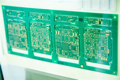
A PCB is a flat board that physically supports and electrically connects electronic components using conductive pathways, tracks, or signal traces etched from copper sheets laminated onto a non-conductive substrate. The assembly process involves several steps, each critical to ensuring the functionality and reliability of the final product.
The first step in PCB assembly is the design phase, where engineers create a schematic diagram that outlines the electronic circuit.
This schematic is then translated into a layout design using specialized software, which determines the placement of components and the routing of electrical connections. Once the design is finalized, the PCB is manufactured, typically involving the etching of copper layers and the application of a solder mask to protect the traces.
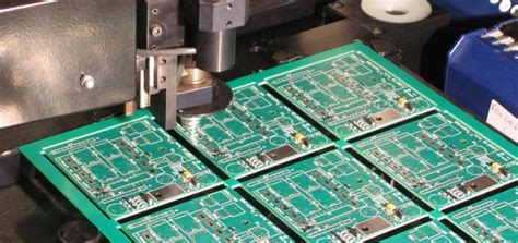
Following the manufacturing of the PCB, the next phase is component placement.
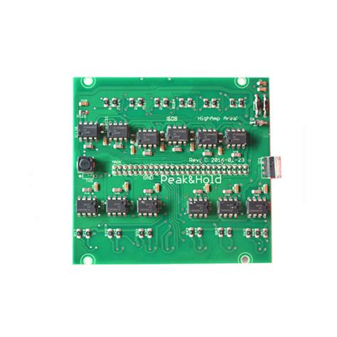
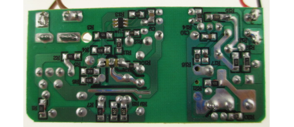
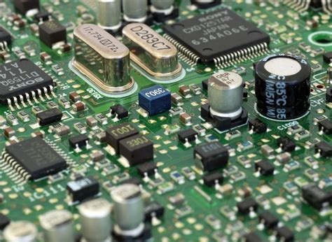
This involves placing various electronic components, such as resistors, capacitors, and integrated circuits, onto the board. Components can be mounted using two primary methods: through-hole technology (THT) and surface-mount technology (SMT). THT involves inserting component leads through pre-drilled holes on the PCB and soldering them on the opposite side, providing strong mechanical bonds. In contrast, SMT allows components to be mounted directly onto the surface of the PCB, offering advantages in terms of space efficiency and automation.
Once the components are placed, the soldering process begins.
Soldering is the technique used to join the components to the PCB by melting solder, a metal alloy, to create a strong electrical connection. For SMT, reflow soldering is commonly used, where the entire board is passed through an oven to melt the solder paste applied during component placement. For THT, wave soldering is often employed, where the board is passed over a wave of molten solder to secure the components.
After soldering, the assembled PCB undergoes inspection and testing to ensure quality and functionality.
Visual inspections, automated optical inspections (AOI), and X-ray inspections are used to detect any defects such as misaligned components or soldering issues. Functional testing is also conducted to verify that the PCB operates as intended, often involving the use of test jigs and software to simulate real-world conditions.
In conclusion, understanding the basics of PCB assembly involves familiarizing oneself with the design, component placement, soldering, and testing processes. Each step is integral to producing a reliable and functional electronic device. As technology continues to advance, the methods and materials used in PCB assembly are constantly evolving, making it an exciting and dynamic field. For beginners, gaining a solid grasp of these fundamentals is the first step towards mastering the art and science of electronics manufacturing.
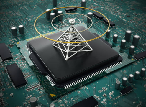
The Role Of Surface Mount Technology In Modern PCB Assembly
Surface Mount Technology (SMT) has revolutionized the field of printed circuit board (PCB) assembly, playing a pivotal role in the advancement of modern electronics. As the demand for smaller, more efficient, and highly reliable electronic devices continues to grow, SMT has emerged as a critical component in meeting these requirements. This technology, which involves mounting electronic components directly onto the surface of PCBs, offers numerous advantages over traditional through-hole technology, thereby shaping the future of electronic manufacturing.
One of the primary benefits of SMT is its ability to significantly reduce the size and weight of electronic assemblies.
By eliminating the need for drilling holes through the board, SMT allows for a more compact design, enabling the production of smaller and lighter devices. This is particularly important in industries such as consumer electronics, where there is a constant push for miniaturization. Moreover, the reduced size of SMT components allows for higher component density on the PCB, which in turn enhances the functionality and performance of the device.
In addition to size reduction, SMT also contributes to improved manufacturing efficiency.
The automation of the SMT process allows for faster assembly times compared to manual through-hole assembly. Automated pick-and-place machines can accurately position thousands of components per hour, significantly increasing production throughput. This efficiency not only reduces manufacturing costs but also shortens the time-to-market for new products, providing a competitive edge in the fast-paced electronics industry.
Furthermore, SMT enhances the reliability and performance of electronic devices.
The shorter interconnections in SMT assemblies result in lower inductance and resistance, which improves signal integrity and reduces the likelihood of electromagnetic interference. This is crucial in high-frequency applications where signal quality is paramount. Additionally, the robust mechanical connection between the component and the PCB surface enhances the durability of the assembly, making it more resistant to mechanical stress and vibration.
Despite these advantages, the implementation of SMT does present certain challenges.
The smaller size of SMT components can make them more difficult to handle and inspect, requiring specialized equipment and techniques. Moreover, the reflow soldering process used in SMT can introduce thermal stress, which must be carefully managed to prevent damage to sensitive components. However, ongoing advancements in SMT equipment and processes continue to address these challenges, further solidifying its role in modern PCB assembly.
The integration of SMT with other emerging technologies is also noteworthy.
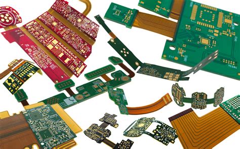
For instance, the combination of SMT with advanced materials and techniques, such as flexible PCBs and 3D printing, is opening new possibilities in electronic design and manufacturing. These innovations are enabling the development of more complex and versatile electronic systems, further expanding the potential applications of SMT.
In conclusion, Surface Mount Technology is a cornerstone of modern PCB assembly, offering significant advantages in terms of size reduction, manufacturing efficiency, and device reliability. As the electronics industry continues to evolve, SMT will undoubtedly remain a key driver of innovation, enabling the development of next-generation electronic devices that meet the ever-increasing demands of consumers and industries alike. Through continuous advancements and integration with other technologies, SMT is poised to maintain its critical role in shaping the future of electronics manufacturing.
Common Challenges In PCB Assembly And How To Overcome Them
Printed Circuit Board (PCB) assembly is a critical process in the electronics manufacturing industry, serving as the backbone for a wide array of electronic devices. However, this process is not without its challenges. Understanding these common challenges and implementing strategies to overcome them is essential for ensuring the reliability and functionality of the final product.
One of the primary challenges in PCB assembly is component placement accuracy.
As electronic devices become more compact and complex, the need for precise placement of components on the PCB becomes increasingly important. Misalignment can lead to poor electrical connections, which may result in device failure. To address this issue, manufacturers can invest in advanced pick-and-place machines equipped with high-resolution cameras and sophisticated software algorithms. These technologies enhance the accuracy of component placement, thereby reducing the likelihood of errors.
Another significant challenge is soldering defects, which can manifest as solder bridges, cold joints, or insufficient solder.
These defects can compromise the electrical integrity of the PCB, leading to malfunctions. To mitigate soldering issues, it is crucial to maintain optimal soldering temperatures and use high-quality solder paste. Additionally, implementing automated optical inspection (AOI) systems can help identify soldering defects early in the assembly process, allowing for timely corrections.
Furthermore, the choice of materials plays a pivotal role in the success of PCB assembly.
The selection of inappropriate materials can lead to issues such as delamination, warping, or thermal stress. To overcome these challenges, manufacturers should carefully evaluate the thermal and mechanical properties of materials to ensure they are suitable for the intended application. Collaborating with material suppliers to obtain detailed specifications and conducting thorough testing can also aid in making informed decisions.
Moreover, managing the complexity of modern PCBs, which often feature multiple layers and intricate designs, presents another challenge.
This complexity can lead to difficulties in routing and signal integrity issues. To address these concerns, designers can utilize advanced PCB design software that offers features such as automated routing and signal integrity analysis.
These tools can help optimize the layout and ensure that the PCB meets the necessary performance criteria. In addition to technical challenges, logistical issues such as supply chain disruptions can impact PCB assembly.
Delays in the availability of components can halt production and extend lead times. To mitigate this risk, manufacturers can establish strong relationships with multiple suppliers and maintain a buffer stock of critical components. Implementing a robust supply chain management system can also enhance visibility and enable proactive decision-making.
Finally, ensuring compliance with industry standards and regulations is a critical aspect of PCB assembly.
Non-compliance can result in product recalls, legal penalties, and damage to the company’s reputation. To overcome this challenge, manufacturers should stay informed about relevant standards and incorporate compliance checks throughout the assembly process.
Regular training for staff on compliance requirements and conducting audits can further ensure adherence to industry standards. In conclusion, while PCB assembly presents several challenges, adopting a proactive approach and leveraging advanced technologies can significantly enhance the quality and reliability of the final product. By addressing issues related to component placement, soldering defects, material selection, design complexity, supply chain management, and regulatory compliance, manufacturers can overcome these challenges and achieve successful PCB assembly.

Innovations In PCB Assembly: Trends To Watch In 2024
In the rapidly evolving landscape of electronics manufacturing, printed circuit board (PCB) assembly stands as a cornerstone of technological advancement. As we approach 2024, several innovations in PCB assembly are poised to redefine industry standards and practices. These emerging trends not only promise to enhance efficiency and precision but also aim to address the growing demand for more sustainable and versatile electronic solutions.
One of the most significant trends in PCB assembly is the increasing adoption of automation and robotics.
Automation technologies have been steadily integrated into manufacturing processes, but recent advancements in robotics and artificial intelligence are set to revolutionize PCB assembly lines. By employing sophisticated robotic systems, manufacturers can achieve higher precision and consistency, reducing the margin for human error. Moreover, these systems can operate continuously, significantly boosting production rates and meeting the escalating demand for electronic devices. As a result, companies investing in automation are likely to gain a competitive edge by delivering high-quality products at a faster pace.
In tandem with automation, the rise of the Internet of Things (IoT) is influencing PCB assembly processes.
IoT devices require compact, efficient, and reliable PCBs to function effectively. Consequently, there is a growing emphasis on miniaturization and the development of multi-layered PCBs that can accommodate complex circuitry within a smaller footprint. This trend is driving innovations in materials and design techniques, enabling the production of PCBs that are not only smaller but also more robust and capable of supporting advanced functionalities. As IoT continues to expand across various sectors, from healthcare to smart homes, the demand for innovative PCB solutions will only intensify.
Another pivotal trend is the shift towards environmentally sustainable practices in PCB assembly.
With increasing awareness of environmental issues, manufacturers are exploring ways to minimize waste and reduce the carbon footprint of their operations. This includes the adoption of eco-friendly materials and the implementation of recycling programs for electronic components. Additionally, advancements in soldering techniques, such as the use of lead-free solders, are contributing to more sustainable manufacturing processes. As regulatory pressures mount and consumer preferences shift towards greener products, sustainability will become an integral aspect of PCB assembly.
Furthermore, the integration of advanced testing and inspection technologies is enhancing the quality assurance processes in PCB assembly.
Techniques such as automated optical inspection (AOI) and X-ray inspection are becoming more sophisticated, allowing for the detection of defects and anomalies with greater accuracy. These technologies not only improve the reliability of PCBs but also reduce the time and cost associated with manual inspections. As a result, manufacturers can ensure that their products meet stringent quality standards while maintaining efficient production timelines.
In addition to these technological advancements, the global supply chain dynamics are also influencing PCB assembly trends.
The recent disruptions in supply chains have highlighted the need for greater resilience and flexibility in sourcing materials and components. Consequently, manufacturers are exploring strategies such as localizing production and diversifying their supplier base to mitigate risks and ensure continuity in their operations. This shift towards more resilient supply chains is expected to have a lasting impact on the PCB assembly industry.
In conclusion, the innovations in PCB assembly anticipated for 2024 are set to transform the industry by enhancing automation, supporting IoT advancements, promoting sustainability, improving quality assurance, and strengthening supply chain resilience. As these trends continue to unfold, they will not only shape the future of PCB assembly but also drive broader technological progress across various sectors.