Best pcb designer
Top Features to Look for in the Best PCB Designer Software
When selecting the best PCB (Printed Circuit Board) designer software, it is crucial to consider a range of features that can significantly impact the efficiency and quality of your design process. As technology continues to advance, the demand for sophisticated and reliable PCB design tools has grown, making it essential to identify the key attributes that distinguish superior software from the rest.
One of the primary features to look for is an intuitive user interface.
A well-designed interface can streamline the design process, allowing users to focus on creativity and functionality rather than struggling with complex navigation. This ease of use is particularly important for both novice designers and seasoned professionals who wish to optimize their workflow.
In addition to user-friendliness, robust design capabilities are a hallmark of top-tier PCB designer software.
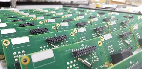
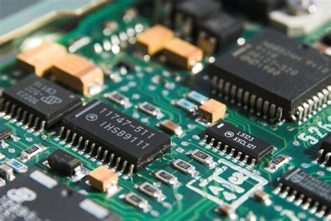
This includes a comprehensive set of tools for schematic capture, layout design, and routing. Advanced routing features, such as auto-router and manual routing options, provide flexibility and precision, enabling designers to create intricate and efficient circuit layouts. Furthermore, the ability to handle multi-layer designs is essential, as modern electronic devices often require complex, compact configurations. The software should also support a wide range of component libraries, ensuring that designers have access to the latest parts and can easily integrate them into their projects.
Another critical feature to consider is the software’s simulation and analysis capabilities.
Effective simulation tools allow designers to test and validate their circuits before physical prototyping, saving time and resources. By simulating the electrical behavior of the circuit, designers can identify potential issues and make necessary adjustments early in the design process. This not only enhances the reliability of the final product but also reduces the likelihood of costly errors. Additionally, thermal and signal integrity analysis tools are invaluable for ensuring that the design will perform optimally under various conditions.
Collaboration features are also increasingly important in today’s interconnected world.
The best PCB designer software should facilitate seamless collaboration among team members, regardless of their geographical location. Cloud-based platforms and version control systems enable multiple users to work on a project simultaneously, ensuring that everyone is on the same page and that changes are tracked efficiently. This collaborative approach not only accelerates the design process but also fosters innovation through the sharing of ideas and expertise.
Moreover, integration with other design and manufacturing tools is a significant advantage.
The ability to export designs in various formats compatible with different manufacturing processes ensures a smooth transition from design to production. This interoperability reduces the risk of errors during manufacturing and helps maintain the integrity of the design throughout the production cycle. Additionally, integration with mechanical design software can facilitate the creation of enclosures and other physical components, providing a holistic approach to product development.
Finally, customer support and community resources are vital considerations when choosing PCB designer software.
Access to responsive technical support can be invaluable when encountering challenges or seeking guidance on complex features. Furthermore, an active user community can provide a wealth of knowledge, offering tips, tutorials, and solutions to common problems. Engaging with a community of users can enhance the learning experience and help designers stay updated with the latest trends and best practices in PCB design.
In conclusion, selecting the best PCB designer software involves evaluating a combination of user interface design, robust design capabilities, simulation and analysis tools, collaboration features, integration options, and support resources. By prioritizing these features, designers can ensure that they have the tools necessary to create innovative, reliable, and efficient electronic products.
Comparing the Best PCB Designers: A Comprehensive Guide
In the rapidly evolving world of electronics, the role of a printed circuit board (PCB) designer is pivotal. As the backbone of electronic devices, PCBs require meticulous design to ensure functionality, reliability, and efficiency. Selecting the best PCB designer can be a daunting task, given the myriad of options available. However, by comparing key attributes and capabilities, one can make an informed decision that aligns with specific project needs.
To begin with, expertise and experience are fundamental criteria when evaluating PCB designers.
A designer with a robust portfolio demonstrates not only technical proficiency but also the ability to adapt to various project requirements. Experienced designers are often adept at troubleshooting potential issues early in the design process, thereby saving time and resources. Furthermore, they are likely to be familiar with industry standards and regulations, ensuring compliance and reducing the risk of costly redesigns.
In addition to experience, the tools and software utilized by a PCB designer are critical.
Advanced design software can significantly enhance the precision and efficiency of the design process. Designers who are proficient in using industry-leading software such as Altium Designer, Eagle, or KiCad are often able to deliver more sophisticated and reliable designs. These tools offer features like 3D visualization, real-time collaboration, and comprehensive libraries, which can streamline the design process and improve the final product’s quality.
Moreover, communication skills are an often-overlooked yet essential aspect of a successful PCB designer.
Effective communication ensures that the designer fully understands the client’s requirements and can provide regular updates throughout the project. This transparency helps in aligning expectations and facilitates a smoother design process. A designer who can articulate complex technical concepts in a clear and concise manner is invaluable, particularly when collaborating with multidisciplinary teams.
Transitioning to another crucial factor, the ability to innovate and adapt to new technologies is a hallmark of the best PCB designers.
The electronics industry is characterized by rapid technological advancements, and designers must be able to incorporate the latest innovations into their work. This adaptability not only enhances the functionality of the final product but also ensures that it remains competitive in the market. Designers who stay abreast of emerging trends and technologies can offer insights and solutions that may not be immediately apparent to others.
Furthermore, cost-effectiveness is a significant consideration when selecting a PCB designer.
While it is tempting to opt for the lowest bid, it is essential to weigh the cost against the quality and reliability of the design. A designer who offers a competitive price while maintaining high standards of quality is often the best choice. It is also worth considering the long-term value of the design, as a well-designed PCB can reduce maintenance costs and extend the product’s lifespan.
In conclusion, choosing the best PCB designer involves a careful evaluation of several factors, including experience, technical proficiency, communication skills, adaptability, and cost-effectiveness. By considering these elements, one can select a designer who not only meets the immediate project requirements but also contributes to the overall success and sustainability of the product. As the demand for innovative and reliable electronic devices continues to grow, the role of skilled PCB designers becomes increasingly vital, underscoring the importance of making an informed choice in this critical area.
How to Choose the Best PCB Designer for Your Project
Selecting the best PCB designer for your project is a critical decision that can significantly impact the success of your electronic product. The process involves evaluating various factors to ensure that the designer you choose can meet your specific needs and deliver a high-quality product. To begin with, it is essential to consider the designer’s experience and expertise.
A seasoned PCB designer will have a comprehensive understanding of the complexities involved in creating efficient and reliable circuit boards.
They will be familiar with the latest industry standards and technologies, which can be crucial for ensuring that your project is up-to-date and competitive.
Moreover, it is important to assess the designer’s portfolio. Reviewing past projects can provide valuable insights into their capabilities and the quality of their work. Look for designs that are similar to your project in terms of complexity and application.
This can give you confidence that the designer has the necessary skills to handle your specific requirements.
Additionally, consider seeking references or testimonials from previous clients. This feedback can offer a more personal perspective on the designer’s reliability, communication skills, and ability to meet deadlines.
Another critical factor to consider is the designer’s familiarity with the specific software tools required for your project.
Different projects may necessitate the use of specialized design software, and a designer who is proficient in these tools can streamline the design process and reduce the likelihood of errors. Furthermore, it is beneficial to choose a designer who is adaptable and willing to learn new tools if necessary, as this flexibility can be advantageous in a rapidly evolving technological landscape.
Cost is also an important consideration when choosing a PCB designer.
While it may be tempting to opt for the lowest bid, it is crucial to balance cost with quality. A designer who offers a significantly lower price may cut corners or lack the experience needed to deliver a high-quality product. Instead, aim for a designer who provides a reasonable quote that reflects their expertise and the complexity of your project. It is also wise to discuss payment terms and ensure that there is a clear understanding of the project’s scope and deliverables to avoid any misunderstandings later on.
Communication is another key aspect to consider. A good PCB designer should be able to clearly articulate their ideas and provide regular updates on the project’s progress.
This transparency can help build trust and ensure that any potential issues are addressed promptly. Additionally, effective communication can facilitate collaboration, allowing you to provide input and feedback throughout the design process.
Finally, consider the designer’s ability to innovate and problem-solve. The best PCB designers are not only technically proficient but also creative thinkers who can devise innovative solutions to complex challenges. This ability can be particularly valuable if your project involves unique requirements or constraints.
In conclusion, choosing the best PCB designer for your project involves a careful evaluation of their experience, portfolio, software proficiency, cost, communication skills, and problem-solving abilities. By taking the time to thoroughly assess these factors, you can select a designer who will not only meet your expectations but also contribute to the overall success of your project.
The Future of PCB Design: Innovations from the Best Designers
In the rapidly evolving world of electronics, printed circuit boards (PCBs) serve as the backbone of modern technology, facilitating the connection and communication between various electronic components. As the demand for more compact, efficient, and powerful devices continues to grow, the role of PCB designers becomes increasingly crucial.
The best PCB designers are not only keeping pace with these demands but are also pioneering innovations that are shaping the future of the industry.
By leveraging cutting-edge technologies and methodologies, these designers are pushing the boundaries of what is possible in PCB design.
One of the most significant innovations in PCB design is the integration of advanced materials.
Traditional PCBs are typically made from fiberglass and epoxy, but the best designers are now exploring the use of materials such as ceramics and flexible polymers. These materials offer superior thermal management, increased flexibility, and enhanced durability, which are essential for the development of next-generation electronic devices. By incorporating these advanced materials, designers can create PCBs that are not only more reliable but also capable of supporting higher performance levels.
In addition to material advancements, the best PCB designers are also embracing the power of automation and artificial intelligence (AI).
Automation tools are streamlining the design process, allowing designers to focus on more complex and creative aspects of their work. AI, in particular, is revolutionizing PCB design by enabling predictive analysis and optimization. Through machine learning algorithms, AI can analyze vast amounts of data to predict potential design flaws and suggest improvements, significantly reducing the time and cost associated with prototyping and testing.
Moreover, the trend towards miniaturization in electronics has led to the development of more compact and efficient PCB designs.
The best designers are adept at utilizing techniques such as high-density interconnect (HDI) technology, which allows for more components to be placed on a smaller board without compromising performance. This is particularly important in industries such as consumer electronics and medical devices, where space is at a premium. By mastering these techniques, designers are able to meet the growing demand for smaller, more powerful devices.
Furthermore, the rise of the Internet of Things (IoT) has introduced new challenges and opportunities for PCB designers.
IoT devices require PCBs that are not only compact but also capable of wireless communication and energy efficiency. The best designers are addressing these challenges by incorporating features such as embedded antennas and energy-harvesting technologies into their designs. This ensures that IoT devices can operate effectively in a wide range of environments while maintaining low power consumption.
As we look to the future, sustainability is becoming an increasingly important consideration in PCB design.
The best designers are leading the charge in developing eco-friendly PCBs by utilizing recyclable materials and designing for disassembly. This approach not only reduces the environmental impact of electronic waste but also aligns with the growing consumer demand for sustainable products.
In conclusion, the future of PCB design is being shaped by the innovative efforts of the best designers in the field. Through the integration of advanced materials, the adoption of automation and AI, the mastery of miniaturization techniques, and a commitment to sustainability, these designers are setting new standards for what is possible in PCB design. As technology continues to advance, the contributions of these pioneering designers will undoubtedly play a pivotal role in the development of the next generation of electronic devices.