Bga pcb assembly
Understanding The Basics Of BGA PCB Assembly
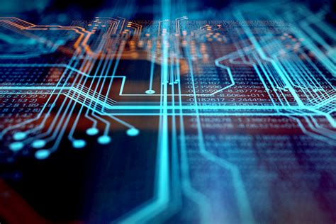
Ball Grid Array (BGA) technology has become a cornerstone in the field of printed circuit board (PCB) assembly, offering a compact and efficient solution for mounting integrated circuits. Understanding the basics of BGA PCB assembly is crucial for those involved in electronics manufacturing and design, as it plays a pivotal role in the performance and reliability of modern electronic devices.
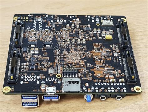
To begin with, BGA is a type of surface-mount packaging used for integrated circuits.
Unlike traditional packages that use pins, BGA packages utilize an array of solder balls on the underside of the device. This configuration allows for a higher density of connections, which is essential as electronic devices continue to shrink in size while increasing in functionality. The solder balls serve as the connection points between the chip and the PCB, providing both electrical connectivity and mechanical support.
The process of BGA PCB assembly involves several critical steps, each requiring precision and attention to detail.
Initially, the PCB is prepared with a solder paste, which is applied to the pads where the BGA will be mounted. This paste is typically a mixture of powdered solder and flux, which helps to clean the surfaces and improve the flow of solder during the reflow process. Once the solder paste is applied, the BGA component is carefully placed onto the PCB, aligning the solder balls with the corresponding pads.
Following placement, the assembly undergoes a reflow soldering process.
During reflow, the entire assembly is heated in a controlled environment, causing the solder balls to melt and form solid connections between the BGA and the PCB. This step is critical, as improper reflow can lead to issues such as solder bridging or insufficient solder joints, which can compromise the functionality of the device. Therefore, precise temperature control and timing are essential to ensure a successful reflow process.
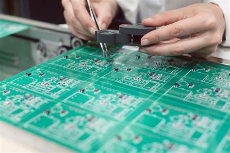
Moreover, inspection and testing are integral parts of BGA PCB assembly.
Due to the hidden nature of the solder joints beneath the BGA package, traditional visual inspection methods are often inadequate. Instead, advanced techniques such as X-ray inspection are employed to verify the integrity of the solder joints. This non-destructive testing method allows for the detection of defects such as voids, misalignments, or incomplete soldering, which could lead to failures in the field.
In addition to inspection, functional testing is conducted to ensure that the assembled PCB meets the required specifications and performance standards.
This step involves powering the device and running a series of tests to verify that all components are operating correctly. Any issues identified during testing can be addressed through rework processes, although these can be challenging and costly, particularly for BGA assemblies.
In conclusion, BGA PCB assembly is a complex process that demands a high level of expertise and precision. From the initial application of solder paste to the final testing and inspection, each step must be carefully executed to ensure the reliability and performance of the finished product. As technology continues to advance, the importance of understanding and mastering BGA PCB assembly will only grow, making it an essential area of knowledge for professionals in the electronics industry.
Common Challenges In BGA PCB Assembly And How To Overcome Them
Ball Grid Array (BGA) technology has become a cornerstone in modern electronics, offering a compact and efficient solution for mounting integrated circuits on printed circuit boards (PCBs). However, the assembly of BGA components presents several challenges that can impact the performance and reliability of electronic devices. Understanding these challenges and implementing effective strategies to overcome them is crucial for manufacturers aiming to maintain high-quality standards in PCB assembly.
One of the primary challenges in BGA PCB assembly is the alignment of the BGA package with the PCB pads.
Due to the array of solder balls located beneath the package, visual inspection is not feasible, making precise alignment critical. Misalignment can lead to open circuits or short circuits, which can compromise the functionality of the device. To address this issue, manufacturers often employ advanced placement machines equipped with vision systems that ensure accurate alignment. Additionally, using solder paste with appropriate viscosity can help in maintaining the position of the BGA during the reflow process.
Another significant challenge is the soldering process itself.
The reflow soldering process must be carefully controlled to ensure that all solder balls melt and form reliable connections without causing defects such as voids or bridging. Voids, which are air pockets trapped within the solder joint, can weaken the mechanical and electrical integrity of the connection. To minimize void formation, it is essential to optimize the reflow profile, including the temperature and time settings, to ensure complete outgassing of volatile compounds in the solder paste. Furthermore, selecting a solder paste with low voiding characteristics can also contribute to reducing this issue.
Thermal management during the reflow process is another critical aspect that can pose challenges.
BGA packages often have high thermal mass, which can lead to uneven heating and cooling rates across the PCB. This can result in thermal stress and warping, potentially causing defects in the solder joints. To mitigate these effects, manufacturers can use thermal profiling to ensure uniform temperature distribution across the board. Additionally, employing a multi-zone reflow oven allows for precise control of temperature gradients, reducing the risk of thermal-related defects.
Inspection and testing of BGA assemblies present further challenges due to the hidden nature of the solder joints
. Traditional visual inspection methods are inadequate, necessitating the use of advanced techniques such as X-ray inspection and automated optical inspection (AOI). X-ray inspection provides a non-destructive means to evaluate the quality of solder joints, allowing for the detection of defects such as voids, misalignment, and insufficient solder. AOI systems, on the other hand, can be used to inspect the surface of the PCB for any visible defects, complementing the insights gained from X-ray analysis.
In conclusion, while BGA PCB assembly presents several challenges, understanding these issues and implementing appropriate solutions can significantly enhance the reliability and performance of electronic devices. By leveraging advanced placement and inspection technologies, optimizing the reflow process, and ensuring effective thermal management, manufacturers can overcome the inherent difficulties associated with BGA assembly. As technology continues to evolve, staying abreast of the latest advancements in assembly techniques will be essential for maintaining competitiveness in the electronics manufacturing industry.
Innovations In BGA PCB Assembly Technology
Ball Grid Array (BGA) technology has become a cornerstone in the field of printed circuit board (PCB) assembly, offering significant advantages in terms of performance and miniaturization. As the demand for more compact and efficient electronic devices continues to rise, innovations in BGA PCB assembly technology are playing a crucial role in meeting these needs. These advancements are not only enhancing the capabilities of electronic devices but also addressing some of the challenges traditionally associated with BGA assembly.
One of the most notable innovations in BGA PCB assembly is the development of advanced soldering techniques.
Traditional soldering methods often faced difficulties in ensuring reliable connections due to the hidden nature of BGA joints. However, the introduction of techniques such as laser soldering and reflow soldering with nitrogen atmospheres has significantly improved the reliability of these connections. These methods provide better control over the soldering process, reducing the risk of defects such as voids and incomplete solder joints. Consequently, these advancements have led to higher yields and improved performance in electronic assemblies.
In addition to soldering techniques, the materials used in BGA assembly have also seen significant improvements.
The development of lead-free solder alloys, driven by environmental regulations and the need for more sustainable manufacturing practices, has been a major focus. These new alloys not only comply with environmental standards but also offer enhanced mechanical properties and thermal performance. This shift towards lead-free materials has necessitated adjustments in the assembly process, but it has ultimately resulted in more robust and reliable electronic products.
Moreover, inspection and testing technologies have evolved to keep pace with the complexities of BGA assemblies.
Traditional inspection methods, such as visual inspection, are inadequate for BGA components due to their concealed solder joints. As a result, advanced techniques like X-ray inspection and automated optical inspection (AOI) have become essential. These technologies allow for non-destructive testing and provide detailed insights into the quality of solder joints, enabling manufacturers to identify and rectify defects early in the production process. This proactive approach not only enhances product quality but also reduces costs associated with rework and returns.
Furthermore, the integration of machine learning and artificial intelligence (AI) into BGA PCB assembly processes is revolutionizing the industry.
These technologies are being used to optimize various aspects of the assembly process, from component placement to defect detection. By analyzing vast amounts of data, AI systems can identify patterns and predict potential issues, allowing for real-time adjustments and continuous improvement. This level of automation and intelligence is leading to more efficient production lines and higher-quality products.
In conclusion, innovations in BGA PCB assembly technology are driving significant advancements in the electronics industry. From improved soldering techniques and materials to advanced inspection methods and the integration of AI, these developments are addressing the challenges associated with BGA assemblies and enhancing the performance and reliability of electronic devices. As technology continues to evolve, it is likely that further innovations will emerge, continuing to push the boundaries of what is possible in PCB assembly. These advancements not only meet the current demands for miniaturization and efficiency but also pave the way for future technological breakthroughs.
Quality Control Techniques In BGA PCB Assembly
In the realm of electronics manufacturing, Ball Grid Array (BGA) technology has emerged as a pivotal component in the assembly of printed circuit boards (PCBs). As devices become increasingly compact and complex, the demand for efficient and reliable BGA PCB assembly has surged. Central to achieving this efficiency and reliability is the implementation of rigorous quality control techniques. These techniques ensure that the final product not only meets the required specifications but also functions optimally in its intended application.
To begin with, one of the most critical quality control techniques in BGA PCB assembly is the inspection of solder joints
. Given the concealed nature of BGA connections, traditional visual inspection methods are inadequate. Instead, advanced imaging technologies such as X-ray inspection are employed. X-ray inspection allows for the non-destructive examination of solder joints, providing detailed images that reveal potential defects such as voids, misalignments, or insufficient solder. By identifying these issues early in the assembly process, manufacturers can take corrective actions before the product reaches the end-user, thereby enhancing the overall reliability of the device.
In addition to X-ray inspection, automated optical inspection (AOI) systems play a significant role in quality control.
Although AOI is more commonly associated with surface-mounted devices, it is also applicable in BGA assembly for inspecting the placement accuracy of components before reflow soldering. AOI systems utilize high-resolution cameras and sophisticated algorithms to detect misplacements, missing components, or incorrect orientations. By ensuring that each component is correctly positioned, AOI systems help prevent assembly errors that could lead to functional failures.
Another essential quality control technique is the implementation of thermal profiling during the reflow soldering process.
Reflow soldering is a critical step in BGA PCB assembly, where precise temperature control is paramount to achieving strong and reliable solder joints. Thermal profiling involves monitoring the temperature of the PCB and its components throughout the reflow process to ensure that the solder paste melts and solidifies correctly. By optimizing the thermal profile, manufacturers can minimize the risk of defects such as solder bridging or cold solder joints, which can compromise the performance of the final product.
Furthermore, electrical testing is a vital component of quality control in BGA PCB assembly.
Techniques such as in-circuit testing (ICT) and functional testing are employed to verify the electrical integrity and functionality of the assembled PCB. ICT involves testing individual components and connections on the PCB to ensure they meet specified electrical parameters. Functional testing, on the other hand, evaluates the performance of the entire assembly under simulated operating conditions. By conducting these tests, manufacturers can identify and rectify any electrical issues before the product is deployed.
Moreover, process control and continuous improvement are integral to maintaining high-quality standards in BGA PCB assembly.
By implementing statistical process control (SPC) methods, manufacturers can monitor and control the assembly process, identifying trends and variations that may indicate potential quality issues. Continuous improvement initiatives, such as root cause analysis and corrective action plans, further enhance the quality control process by addressing the underlying causes of defects and preventing their recurrence.
In conclusion, quality control techniques in BGA PCB assembly are multifaceted and encompass a range of advanced technologies and methodologies. From X-ray and optical inspections to thermal profiling and electrical testing, each technique plays a crucial role in ensuring the reliability and performance of the final product. By integrating these techniques into the assembly process, manufacturers can deliver high-quality PCBs that meet the ever-evolving demands of modern electronic devices.