Understanding Board PCBA: Essential Insights and Best Practices
Key Takeaways
In understanding board PCBA, it’s essential to grasp the fundamental principles and methodologies that underpin this intricate field. One of the most critical aspects of pcb assembly is the collaborative synergy between design, manufacturing, and testing processes. Efficient pcba development begins with a thorough design phase, where attention to detail in layout and component selection can significantly influence the overall performance and reliability of the assembly.
Manufacturing techniques play a crucial role in ensuring that the printed circuit board assemblies are produced with precision. This includes selecting the right soldering methods, such as surface mount technology (SMT) or through-hole technology, which directly impacts the final product’s quality and longevity. Furthermore, stringent quality control measures must be implemented throughout the entire pcb assembly process to detect any discrepancies early on, ensuring that each component functions optimally within its intended application.
Ultimately, having a solid foundation in these areas not only helps mitigate common challenges faced during pcba but also prepares designers and engineers to adopt innovative strategies as advancements continue in this dynamic industry. Familiarity with best practices and emerging trends will empower professionals to enhance their assemblies’ performance while remaining competitive in today’s rapidly evolving technological landscape.
Introduction to Board PCBA: Key Concepts and Terminology
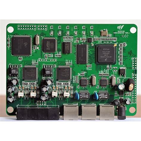
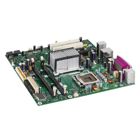
Understanding Board PCBA—short for Printed Circuit Board Assembly—is essential for anyone involved in electronics design and manufacturing. A PCBA is essentially the process of soldering electronic components onto a printed circuit board, creating a functional assembly. This process may seem straightforward, but it involves a range of intricate steps and terminologies that are crucial to grasp for successful implementation.
Key concepts in PCB assembly include the components involved, such as resistors, capacitors, and integrated circuits. It’s paramount to be familiar with both surface-mount technology (SMT) and through-hole technology (THT), which are two primary methods of assembling components onto the board. Each method has its own advantages and situational benefits depending on design requirements and space constraints.
Moreover, awareness of common terms associated with PCBA is vital. Terms like silkscreen, solder mask, and vias are fundamental in understanding how components communicate within the circuit. Engaging with these key concepts sets a solid foundation for diving deeper into the more complex aspects of design and manufacturing.
“A clear grasp of terminology not only enhances communication among team members but also plays a pivotal role in ensuring that the design specifications are accurately met.”
Furthermore, familiarity with industry standards—such as IPC-A-610 for acceptability of electronic assemblies—helps ensure quality throughout the board assembly process. This baseline knowledge ultimately supports engineers and manufacturers in optimizing their workflow while minimizing errors, making it indispensable to any professional’s toolkit in the field of electronics.
As you explore further into this article, you’ll discover best practices that enhance your approach to PCB assembly, improving both efficiency and quality in your projects.
The Design Process: Best Practices for Board PCBA Development
The design process for pcb assembly is a critical phase that lays the foundation for successful PCBA outcomes. A well-executed design ensures functionality, manufacturability, and reliability of the final product. Here are several best practices to consider during the development stage:
Define Objectives Clearly: Establishing clear objectives at the outset helps streamline the design process. Identify specific requirements such as size, weight, connectivity, and environmental conditions to guide the design decisions.
Select Appropriate Materials: The choice of materials is pivotal in determining the performance of the printed circuit board assembly. Ensure that you choose high-quality substrates and components that meet both durability and performance standards.
Utilize Design Software Effectively: Employ advanced PCB design software that supports features like 3D modeling, which enhances visualization and identifies potential issues early in the process. Tools that automate tasks can also reduce errors and save time.
Implement a Layered Approach: When designing multilayer boards, carefully manage layer stack-ups to optimize signal integrity and reduce electromagnetic interference (EMI). Following established stacking conventions can prevent future problems during manufacturing.
Create Comprehensive Documentation: Proper documentation is essential for effective communication among stakeholders involved in both design and manufacturing processes. Include diagrams, specifications, and assembly instructions to facilitate a smoother workflow.
Engage in Design Reviews: Regularly conduct design reviews that involve cross-functional teams to gain multiple perspectives on potential issues or opportunities for improvement early in development.
Prioritize Design for Manufacturability (DFM): Integrate DFM principles into your PCB layout by designing with manufacturing processes in mind, which helps minimize costs while maximizing output quality.
Prototype Early and Often: Creating prototypes during different stages of development allows designers to assess functionality and address issues before mass production begins.
By adhering to these best practices, you can enhance the efficiency of your pcb assembly process while ensuring high-performance standards are met for your final product. Embracing a proactive approach to design considerations significantly contributes to minimizing challenges later in manufacturing and testing phases.
| Considerations | Description |
|---|---|
| Objectives | Clearly define size, weight, connectivity requirements |
| Materials | Choose high-quality substrates/components |
| Software | Utilize advanced design software with 3D modeling capabilities |
| Layer Management | Optimize signal integrity through careful layer stack-ups |
| Documentation | Provide comprehensive documentation for smooth communication |
| Design Reviews | Engage in regular cross-functional team reviews |
| DFM Principles | Integrate manufacturability principles into your PCB layout |
| Prototyping | Prototype throughout development stages to assess functionality |
By following these guidelines, you can foster a streamlined development process for your Board PCBA projects that leads to successful outcomes where quality meets functionality.
Manufacturing Techniques: Understanding the PCB Assembly Process
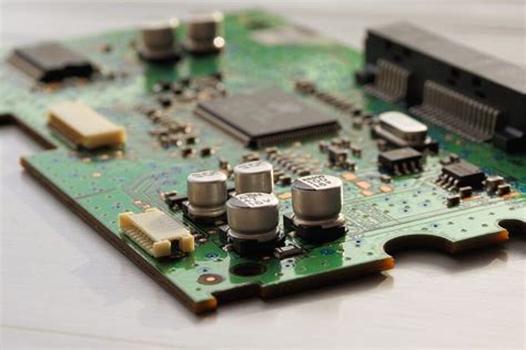
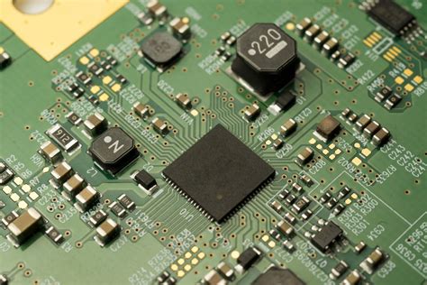
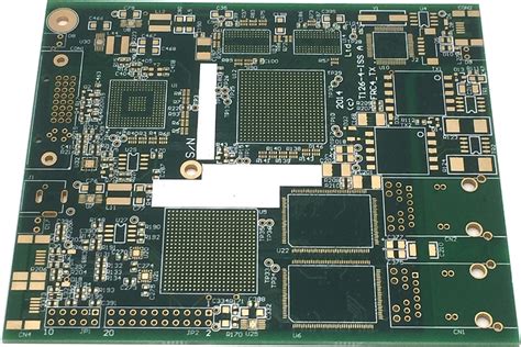
The pcb assembly process is a critical aspect of producing high-quality electronic devices, and understanding the various manufacturing techniques involved is essential for any engineer or manufacturer. At its core, pcba refers to the process where electronic components are mounted onto a printed circuit board (PCB) to create functioning circuitry. This assembly can occur using several methodologies, including surface mount technology (SMT) and through-hole technology (THT). Each technique comes with its own set of advantages and applications.
In surface mount technology, components are soldered directly onto the surface of the PCB, allowing for a more compact design and shorter production times. This is particularly beneficial for modern electronics that require smaller size and higher efficiency. In contrast, through-hole technology, which involves inserting component leads through pre-drilled holes in the PCB, provides stronger mechanical connections and is often favored for more robust applications or components that require additional support.
Furthermore, the implementation of automated assembly machinery has significantly improved precision and speed in pcb assembly. However, even with automation, skilled technicians are vital to oversee operations and ensure quality throughout each stage of production. Careful consideration must be given to aspects such as solder paste application, component placement accuracy, and reflow processes—all of which are critical to achieving a successful and reliable pcba. As you delve deeper into these manufacturing techniques, you’ll discover how various factors influence the overall efficacy of board assembly, from initial design choices to final quality assurance tests. Understanding these intricacies will empower manufacturers to optimize their processes effectively.
Quality Control: Ensuring Reliability in Board PCBA
Ensuring the reliability of pcb assembly is paramount, as it directly impacts the performance and longevity of electronic devices. Quality control processes play a crucial role in validating that each step of the pcba lifecycle meets stringent standards. This begins with thorough inspection during the design phase, where potential issues such as layout errors or component placement misalignments are identified early. Following the design approval, manufacturing techniques must be closely monitored; from soldering methods to materials used, each element is critical in maintaining quality.
Implementing automated optical inspection (AOI) and X-ray systems during production can significantly enhance detection rates for defects such as solder joint integrity and component misplacement. Additionally, continuous feedback loops from testing phases need to be established to ensure that any anomalies are addressed promptly. By embracing a culture of continuous improvement, organizations can refine their processes, leading to higher yields and reduced costs associated with rework or returns. Ultimately, maintaining high standards in quality control not only ensures reliability in pcba, but also builds a foundation for trust with customers and partners alike.
Testing Methods: Validating Functionality and Performance
Testing is a crucial stage in the pcb assembly process, ensuring that every component on the board operates as intended. Various pcba testing methods exist, tailored to different factors such as complexity, cost, and specific performance criteria. One of the most common methods is the Functional Testing, which involves checking each function of the assembled PCB to ensure it corresponds with the design specifications. This type of testing can catch errors early in the manufacturing process, minimizing defects and ensuring reliability.
In addition to functional checks, In-Circuit Testing (ICT) plays a significant role in assessing individual components’ functionality while still on the assembly line. This method employs specialized probes that make direct contact with locations on the board, effectively measuring voltages and ensuring proper assembly of components. Furthermore, Automated Optical Inspection (AOI) leverages advanced imaging technology to identify potential manufacturing defects visually, such as missed solder joints or misplaced components.
Moreover, stress testing is another pivotal approach that evaluates how well a pcba withstands extreme conditions. This includes thermal cycling and vibration tests that simulate real-world applications and environmental factors the board may encounter during its lifespan. Piloting these tests can prevent future failures by allowing engineers to detect weaknesses in design or materials.
Ultimately, adopting a well-rounded strategy combining these testing methods ensures that the pcb assembly not only meets performance standards but also guarantees durability and quality. With rigorous testing in place, manufacturers can confidently deliver reliable products that meet customer expectations while paving the way for successful device deployment in various applications.
Common Challenges in Board PCBA and How to Overcome Them
In the realm of pcb assembly, several obstacles frequently arise, impacting both the efficiency and efficacy of the process. One prevalent issue is design complexity, which can lead to difficulties in achieving optimal performance. Engineers often encounter challenges related to signal integrity and thermal management, necessitating a thorough understanding of the underlying principles during the design phase. To mitigate these problems, it’s essential to adopt best practices such as modular design approaches and extensive simulation before production.
Another significant challenge is component placement during assembly. If components are not placed accurately, it can result in malfunctioning boards or increased rework efforts. Utilizing automated soldering techniques and employing advanced optical inspection systems can greatly enhance precision in this regard.
Moreover, sourcing quality materials poses a continuous challenge in the pcba process. Variability in component quality can lead to failures post-assembly. Establishing strong relationships with reliable suppliers and conducting thorough material inspections before assembly are effective strategies to ensure high-quality outcomes.
Finally, maintaining stringent quality control standards throughout the production stages is critical. For instance, implementing regular checks and balances, along with statistical process control techniques, can help identify defects early on—reducing costs associated with last-minute fixes or redesigns. By addressing these common challenges proactively, companies can significantly improve their overall board PCBA production quality and reliability while fostering innovation within their processes.
Future Trends in PCB Assembly: Innovations and Advancements
The realm of pcb assembly is witnessing a wave of innovations and advancements that are set to transform the industry landscape. As technology continues to evolve, several trends are emerging that will shape the future of printed circuit board assembly (PCBA). One significant trend is the increasing adoption of automation in the manufacturing process. Facilities are investing in advanced robotics and AI-driven systems, which enhance efficiency and accuracy in assembly, reducing human error and speeding up production times. Another vital advancement is the growing focus on sustainability. Manufacturers are prioritizing eco-friendly materials and processes, striving to mitigate environmental impact while meeting regulatory standards.
Moreover, miniaturization of components is paving the way for more compact designs, allowing for smaller devices with enhanced functionalities. This trend necessitates a re-evaluation of traditional pcb assembly techniques as engineers seek innovative solutions to handle intricate layouts without compromising performance. Additionally, advancements in 3D printing technology are revolutionizing prototyping methods, facilitating rapid design iterations and lowering costs significantly.
Furthermore, there is a clear shift towards adopting more robust quality control measures powered by data analytics and real-time monitoring systems. These enhancements allow for improved reliability in PCBA, ensuring that products meet stringent quality standards before reaching consumers. Collectively, these trends highlight an exciting future for PCB assembly that not only capitalizes on technological advancements but also fosters a commitment to sustainability and quality excellence.
Conclusion
In summary, understanding board PCBA is vital for anyone involved in the field of electronics. Throughout this article, we’ve explored various facets of pcb assembly, ranging from the initial design process to the manufacturing techniques that ensure high-quality outputs. Emphasizing best practices in PCBA development, we’ve highlighted how thoughtful design choices can significantly enhance the reliability and functionality of printed circuit boards. Quality control remains a key focus; rigorous methods must be employed to evaluate each assembly stage to guarantee that products meet stringent standards before reaching the market. Furthermore, we have acknowledged common challenges in pcba, offering insights into how these obstacles can be effectively addressed through innovative solutions and collaboration among teams. As technology continues to evolve, staying updated on future trends in pcb assembly will be crucial for adapting and thriving in this dynamic industry. Ultimately, a robust understanding of these concepts will equip professionals with the tools needed to succeed in their projects and foster advancements within electronic practices.
FAQs
What is PCB assembly (PCBA)?
PCB assembly, commonly referred to as PCBA, is the process of combining a printed circuit board (PCB) with electronic components to create a functional electronic circuit.
What are the main steps involved in the PCB assembly process?
The main steps in pcb assembly include design and layout of the PCB, printing of the circuit pattern, placement of electronic components, soldering, and testing to ensure functionality.
Why is quality control important in board PCBA?
Quality control is crucial in board PCBA as it ensures that each assembled unit meets industry standards for reliability and performance. This helps prevent failures in the final product.
What are some common challenges faced during PCBA manufacturing?
Common challenges include misaligned components, solder defects, and issues with material quality. Addressing these can significantly improve the overall success of the pcb assembly process.
How can I ensure efficient testing of my PCB assembly?
Efficient testing can be achieved through various methods such as functional testing, In-Circuit Testing (ICT), and Automated Optical Inspection (AOI). Each method helps validate different aspects of performance in your pcba.
For more detailed insights on PCB assembly techniques and best practices, please click here: Andwin PCB Assembly