Ceramic pcb multilayer
Advantages Of Ceramic PCB Multilayer In High-Frequency Applications
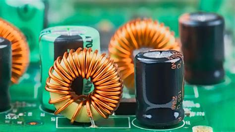
Ceramic PCB multilayer technology has emerged as a pivotal advancement in the realm of high-frequency applications, offering a multitude of advantages that cater to the demanding needs of modern electronic systems. As the demand for high-performance electronic devices continues to escalate, the need for reliable and efficient circuit boards becomes increasingly critical. Ceramic PCBs, particularly in multilayer configurations, have proven to be a superior choice due to their unique properties and capabilities.
One of the foremost advantages of ceramic PCB multilayer technology is its exceptional thermal conductivity.
Unlike traditional materials such as FR-4, ceramic substrates possess a high thermal conductivity, which allows for efficient heat dissipation. This characteristic is particularly beneficial in high-frequency applications where excessive heat generation can lead to performance degradation or even failure of electronic components. By effectively managing heat, ceramic multilayer PCBs ensure the longevity and reliability of the devices they support.
In addition to thermal management, ceramic PCBs offer excellent electrical insulation properties.
This is crucial in high-frequency applications where signal integrity is paramount. The dielectric properties of ceramic materials minimize signal loss and crosstalk, thereby enhancing the overall performance of the circuit. Furthermore, the low dielectric constant of ceramics contributes to reduced signal delay, which is essential for maintaining the speed and efficiency of high-frequency operations.
Moreover, ceramic PCB multilayer technology provides superior mechanical strength and stability.
The inherent rigidity of ceramic materials ensures that the circuit boards can withstand mechanical stresses and environmental factors without compromising their structural integrity. This robustness is particularly advantageous in applications that require durability and reliability, such as aerospace, automotive, and telecommunications industries. The ability to maintain performance under harsh conditions makes ceramic multilayer PCBs an ideal choice for critical applications.
Another significant advantage of ceramic PCB multilayer technology is its capability to support miniaturization.
As electronic devices become increasingly compact, the need for smaller and more efficient circuit boards becomes evident. Ceramic multilayer PCBs allow for the integration of multiple layers within a compact footprint, enabling the design of smaller and more complex circuits. This miniaturization capability is essential for the development of advanced electronic devices that require high functionality within limited space.
Furthermore, ceramic PCBs exhibit excellent chemical resistance, making them suitable for use in environments where exposure to corrosive substances is a concern.
This resistance ensures that the circuit boards maintain their performance and reliability over time, even in challenging conditions. The combination of chemical resistance, thermal management, and electrical insulation makes ceramic multilayer PCBs a versatile solution for a wide range of high-frequency applications.
In conclusion, the advantages of ceramic PCB multilayer technology in high-frequency applications are manifold.
From superior thermal conductivity and electrical insulation to mechanical strength and miniaturization capabilities, ceramic PCBs offer a comprehensive solution to the challenges faced by modern electronic systems. As the demand for high-performance and reliable electronic devices continues to grow, the adoption of ceramic multilayer PCBs is likely to increase, driving further innovation and advancement in the field of high-frequency applications. The unique properties of ceramic materials position them as a key enabler of future technological developments, ensuring that electronic systems can meet the ever-evolving demands of the industry.
Manufacturing Process Of Ceramic PCB Multilayer
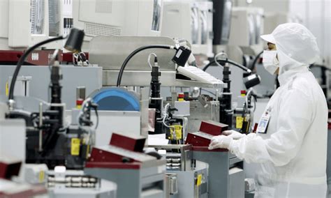
The manufacturing process of ceramic PCB multilayer boards is a sophisticated and intricate procedure that requires precision and expertise. Ceramic PCBs, known for their excellent thermal conductivity and electrical insulation properties, are increasingly used in high-performance electronic applications. The multilayer variant of these boards further enhances their capabilities by allowing for more complex circuit designs and greater functionality within a compact space. Understanding the manufacturing process of ceramic PCB multilayer boards is essential for appreciating their role in modern electronics.
To begin with, the selection of materials is a critical step in the manufacturing process.
Ceramic substrates, typically made from alumina, aluminum nitride, or beryllium oxide, are chosen for their superior thermal and electrical properties. These materials provide a stable base that can withstand high temperatures and offer excellent insulation. Once the appropriate ceramic material is selected, it is prepared for the layering process. This involves cutting the ceramic into thin sheets, which will form the individual layers of the PCB.
Following the preparation of the ceramic sheets, the next step involves the application of conductive materials.
Conductive pastes, often composed of metals such as silver, gold, or copper, are screen-printed onto the ceramic layers. This process requires precision to ensure that the conductive paths are accurately formed, as they will serve as the electrical connections between components. The screen-printing process is repeated for each layer, with careful alignment to ensure that the conductive paths on different layers connect correctly.
Once the conductive paths are applied, the layers are stacked together to form a multilayer structure.
This stacking process is crucial, as it determines the final configuration of the PCB. The layers must be aligned with high precision to ensure that the electrical connections between them are accurate and reliable. To achieve this, advanced alignment techniques and equipment are used, minimizing any potential misalignment that could affect the board’s performance.
After stacking, the multilayer structure undergoes a lamination process.
This involves applying heat and pressure to bond the layers together, creating a single, cohesive unit. The lamination process not only ensures the structural integrity of the PCB but also enhances its thermal and mechanical properties. The resulting laminated board is robust and capable of withstanding the rigors of electronic applications.
Following lamination, the board is subjected to a series of finishing processes.
These include drilling holes for vias and mounting components, as well as applying surface finishes to protect the conductive paths from oxidation and wear. The finishing processes are critical for ensuring the long-term reliability and performance of the PCB.
Finally, the completed ceramic PCB multilayer board undergoes rigorous testing to verify its functionality and quality.
Electrical tests are conducted to ensure that the conductive paths are correctly formed and that there are no short circuits or open connections. Additionally, thermal and mechanical tests may be performed to assess the board’s ability to withstand operational stresses.
In conclusion, the manufacturing process of ceramic PCB multilayer boards is a complex and meticulous procedure that combines advanced materials and precise engineering techniques. Each step, from material selection to final testing, is crucial in producing a high-quality product that meets the demanding requirements of modern electronic applications. As technology continues to advance, the role of ceramic PCB multilayer boards in enabling innovative solutions will undoubtedly grow, underscoring the importance of their sophisticated manufacturing process.

Thermal Management Solutions With Ceramic PCB Multilayer
In the realm of modern electronics, the demand for efficient thermal management solutions has become increasingly critical. As devices become more compact and powerful, the need to dissipate heat effectively is paramount to ensure reliability and longevity. One innovative solution that has emerged to address these challenges is the use of ceramic PCB multilayer technology. This advanced approach offers a myriad of benefits, making it an attractive option for various high-performance applications.
Ceramic PCBs, or printed circuit boards, are distinguished by their use of ceramic materials as the substrate, as opposed to traditional materials like FR-4.
The inherent properties of ceramics, such as high thermal conductivity, low thermal expansion, and excellent electrical insulation, make them particularly well-suited for applications where heat dissipation is a primary concern. By employing a multilayer design, ceramic PCBs can further enhance their thermal management capabilities, providing a robust solution for complex electronic systems.
The multilayer structure of ceramic PCBs allows for the integration of multiple layers of circuitry within a single board.
This design not only increases the density of the circuit but also facilitates the efficient distribution of heat across the board. By strategically placing thermal vias and conductive paths, heat generated by components can be effectively transferred away from critical areas, thereby reducing the risk of overheating and potential failure. Moreover, the ability to incorporate multiple layers enables designers to create more compact and lightweight devices without compromising on performance.
In addition to their superior thermal management properties, ceramic PCB multilayers offer other significant advantages.
For instance, their high mechanical strength and durability make them ideal for use in harsh environments, where traditional PCBs might fail. This resilience is particularly beneficial in industries such as aerospace, automotive, and telecommunications, where reliability is paramount. Furthermore, ceramic materials are inherently resistant to chemical corrosion, adding another layer of protection for sensitive electronic components.
The use of ceramic PCB multilayers also contributes to improved signal integrity and reduced electromagnetic interference (EMI).
The excellent dielectric properties of ceramics help to minimize signal loss and crosstalk, ensuring that electronic signals are transmitted with high fidelity. This is especially important in high-frequency applications, where maintaining signal integrity is crucial for optimal performance. Additionally, the ability to incorporate ground planes and shielding layers within the multilayer structure further mitigates the risk of EMI, enhancing the overall reliability of the system.
Despite these advantages, it is important to acknowledge the challenges associated with ceramic PCB multilayer technology.
The manufacturing process for ceramic PCBs is more complex and costly compared to traditional PCBs, which can be a barrier for some applications. However, as demand for high-performance thermal management solutions continues to grow, advancements in manufacturing techniques are expected to drive down costs and make ceramic PCB multilayers more accessible.
In conclusion, ceramic PCB multilayer technology represents a significant advancement in thermal management solutions for modern electronics. By leveraging the unique properties of ceramics and the benefits of a multilayer design, this approach offers a powerful solution for dissipating heat and enhancing the performance and reliability of electronic devices. As industries continue to push the boundaries of what is possible with technology, the role of ceramic PCB multilayers in meeting these demands is likely to become increasingly prominent.

Innovations In Ceramic PCB Multilayer Technology
Ceramic PCB multilayer technology has emerged as a pivotal innovation in the field of electronics, offering significant advantages over traditional printed circuit boards. This technology is particularly noteworthy for its ability to enhance performance in high-frequency and high-temperature applications, making it indispensable in industries such as aerospace, automotive, and telecommunications. As electronic devices continue to shrink in size while increasing in functionality, the demand for more efficient and reliable circuit boards has intensified, leading to the development and refinement of ceramic PCB multilayer technology.
One of the primary benefits of ceramic PCB multilayer technology is its superior thermal conductivity.
Unlike conventional PCBs, which often rely on organic materials, ceramic PCBs utilize inorganic substrates such as alumina, aluminum nitride, or beryllium oxide. These materials are renowned for their excellent thermal management properties, allowing for efficient heat dissipation. This is particularly crucial in high-power applications where excessive heat can lead to device failure. By effectively managing heat, ceramic PCBs ensure the longevity and reliability of electronic components, thereby reducing the risk of malfunctions and extending the lifespan of devices.
In addition to thermal management, ceramic PCB multilayer technology offers exceptional electrical performance.
The use of ceramic materials results in lower dielectric losses, which is essential for maintaining signal integrity in high-frequency applications. This characteristic is particularly beneficial in telecommunications, where the demand for faster data transmission speeds continues to grow. Furthermore, the inherent rigidity and stability of ceramic materials contribute to the mechanical robustness of the PCBs, making them less susceptible to warping or deformation under stress. This durability is a critical factor in applications where environmental conditions can be harsh or unpredictable.
Moreover, the multilayer aspect of ceramic PCBs allows for greater design flexibility and complexity.
By stacking multiple layers of circuitry, designers can create more compact and intricate designs without compromising performance. This capability is increasingly important as devices become more sophisticated and require more components to be integrated into a limited space. The multilayer design also facilitates the incorporation of various functionalities, such as signal routing, power distribution, and electromagnetic interference shielding, within a single board. This integration not only enhances the overall performance of the device but also simplifies the manufacturing process, leading to cost savings and increased production efficiency.
Despite these advantages, the adoption of ceramic PCB multilayer technology is not without challenges.
The manufacturing process for ceramic PCBs is more complex and costly compared to traditional PCBs, primarily due to the specialized materials and techniques required. However, ongoing research and development efforts are focused on optimizing production methods to reduce costs and improve accessibility. As these advancements continue, it is anticipated that ceramic PCB multilayer technology will become more widely adopted across various industries.
In conclusion, ceramic PCB multilayer technology represents a significant advancement in the realm of electronic circuit design. Its superior thermal and electrical properties, combined with the flexibility offered by multilayer configurations, make it an ideal choice for high-performance applications. While challenges remain in terms of manufacturing complexity and cost, the potential benefits of this technology are undeniable. As innovation continues to drive the evolution of electronic devices, ceramic PCB multilayer technology is poised to play a crucial role in meeting the demands of the future.
Comparing Ceramic PCB Multilayer To Traditional PCB Materials
In the realm of electronic circuit design, the choice of substrate material plays a pivotal role in determining the performance, reliability, and longevity of the final product. Among the various options available, ceramic PCB multilayer technology has emerged as a compelling alternative to traditional PCB materials such as FR-4, polyimide, and metal-core substrates. To understand the advantages and limitations of ceramic PCB multilayers, it is essential to compare them with these conventional materials, considering factors such as thermal management, electrical performance, and mechanical properties.
Ceramic PCB multilayers are renowned for their exceptional thermal conductivity, which is a critical factor in high-power and high-frequency applications.
Unlike traditional materials like FR-4, which have relatively low thermal conductivity, ceramics such as alumina and aluminum nitride can efficiently dissipate heat away from critical components. This capability not only enhances the performance of the electronic device but also extends its operational lifespan by preventing overheating. Consequently, ceramic PCBs are particularly advantageous in applications where thermal management is paramount, such as in LED lighting, power electronics, and RF communication systems.
In addition to superior thermal properties, ceramic PCB multilayers offer excellent electrical performance.
The dielectric properties of ceramic materials are inherently stable over a wide range of temperatures and frequencies, which ensures consistent signal integrity and minimal signal loss. This is in stark contrast to traditional materials like FR-4, which can exhibit significant variations in dielectric constant and loss tangent with temperature changes. As a result, ceramic PCBs are highly suitable for high-frequency applications, including microwave and millimeter-wave circuits, where maintaining signal fidelity is crucial.
Moreover, the mechanical robustness of ceramic PCB multilayers is another distinguishing feature.
Ceramics are inherently rigid and resistant to mechanical stress, making them ideal for environments where the circuit board may be subjected to physical shocks or vibrations. This durability is a significant advantage over traditional materials, which may require additional reinforcement or protective measures to withstand similar conditions. Furthermore, the inherent rigidity of ceramics allows for the fabrication of complex multilayer structures with precise dimensional tolerances, enabling the integration of more components and functionalities within a compact footprint.
However, it is important to acknowledge the limitations of ceramic PCB multilayers.
One of the primary challenges is the cost associated with ceramic materials and the specialized manufacturing processes required. Compared to traditional PCB materials, ceramics can be significantly more expensive, which may be a deterrent for cost-sensitive applications. Additionally, the brittleness of ceramics, while contributing to their rigidity, can also pose a risk of fracture during handling or assembly, necessitating careful design and manufacturing considerations.
Despite these challenges, the benefits of ceramic PCB multilayers often outweigh their drawbacks, particularly in applications where performance and reliability are of utmost importance. As technology continues to advance, the demand for high-performance electronic devices is expected to grow, further driving the adoption of ceramic PCB multilayers. In conclusion, while traditional PCB materials will continue to have their place in the industry, ceramic PCB multilayers offer a compelling alternative for applications that require superior thermal management, electrical performance, and mechanical durability. As such, they represent a significant advancement in the field of electronic circuit design, promising to enhance the capabilities of future electronic systems.