Ceramic pcb via
Advantages Of Using Ceramic PCB Via In High-Frequency Applications
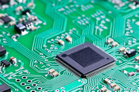
Ceramic printed circuit boards (PCBs) have emerged as a pivotal component in high-frequency applications, offering a range of advantages that make them superior to traditional PCB materials. One of the most significant features of ceramic PCBs is the use of vias, which are conductive pathways that allow electrical connections between different layers of the board. The integration of ceramic PCB vias in high-frequency applications provides numerous benefits, enhancing performance and reliability.
To begin with, ceramic materials possess excellent thermal conductivity, which is crucial in high-frequency applications where heat dissipation is a major concern.
The ability of ceramic PCBs to efficiently conduct heat away from critical components ensures that the system operates within safe temperature limits, thereby enhancing the longevity and reliability of the device. This thermal management capability is further augmented by the use of vias, which facilitate the transfer of heat between layers, preventing hotspots and ensuring uniform temperature distribution across the board.
Moreover, ceramic PCBs exhibit superior electrical insulation properties, which are essential in high-frequency applications to minimize signal loss and interference.
The dielectric constant of ceramic materials is relatively stable over a wide range of frequencies, which helps maintain signal integrity and reduces the risk of crosstalk between adjacent traces. Vias in ceramic PCBs contribute to this by providing a low-loss pathway for signals to traverse between layers, ensuring that high-frequency signals are transmitted with minimal attenuation.
In addition to thermal and electrical advantages, ceramic PCBs are known for their mechanical robustness.
The inherent strength and rigidity of ceramic materials make them resistant to mechanical stress and environmental factors such as moisture and chemical exposure. This durability is particularly beneficial in high-frequency applications where PCBs may be subjected to harsh operating conditions. The use of vias in ceramic PCBs further enhances their mechanical stability by providing additional structural support, reducing the risk of delamination and other mechanical failures.
Furthermore, the miniaturization of electronic components has become a critical trend in modern technology, and ceramic PCBs are well-suited to meet this demand.
The high-density interconnect (HDI) capabilities of ceramic PCBs, facilitated by the use of vias, allow for the integration of more components in a smaller footprint. This is particularly advantageous in high-frequency applications where space is often at a premium, enabling the design of compact and efficient systems without compromising performance.
Another noteworthy advantage of ceramic PCB vias is their compatibility with advanced manufacturing techniques.
The precision and accuracy of modern fabrication processes allow for the creation of vias with tight tolerances, ensuring consistent performance across all connections. This level of precision is essential in high-frequency applications where even minor variations can significantly impact the overall performance of the system.
In conclusion, the use of ceramic PCB vias in high-frequency applications offers a multitude of advantages, including superior thermal management, excellent electrical insulation, mechanical robustness, and support for miniaturization. These benefits make ceramic PCBs an ideal choice for a wide range of high-frequency applications, from telecommunications to aerospace and beyond. As technology continues to evolve, the role of ceramic PCBs and their vias will undoubtedly become even more critical in meeting the demands of increasingly complex and high-performance electronic systems.
Manufacturing Process Of Ceramic PCB Via: A Step-By-Step Guide
The manufacturing process of ceramic PCB vias is a meticulous and intricate procedure that requires precision and expertise. Ceramic PCBs, known for their excellent thermal conductivity and electrical insulation properties, are increasingly used in high-performance electronic applications. The creation of vias, which are essential for establishing electrical connections between different layers of the PCB, involves several critical steps. Understanding this process is crucial for manufacturers aiming to produce high-quality ceramic PCBs.
Initially, the process begins with the selection of the ceramic substrate.
The choice of substrate material is vital, as it influences the thermal and electrical performance of the final product. Common materials include alumina, aluminum nitride, and beryllium oxide, each offering distinct advantages. Once the substrate is selected, it is meticulously cleaned to remove any impurities that could affect the subsequent steps. This cleaning process ensures that the surface is free from contaminants, which is essential for achieving strong adhesion in later stages.
Following the cleaning, the substrate undergoes a drilling process to create the vias.
This step is performed using advanced laser drilling technology, which allows for precise and accurate hole formation. The laser drilling process is preferred over mechanical drilling due to its ability to produce smaller and more consistent holes, which are crucial for high-density applications. The precision of laser drilling ensures that the vias are perfectly aligned, which is essential for maintaining the integrity of the electrical connections.
Once the vias are drilled, the next step involves metallization.
This process is critical as it provides the conductive pathways necessary for electrical connectivity. Typically, a thin layer of metal, such as copper, is deposited onto the walls of the vias. This is achieved through a process known as electroless plating, which involves the chemical deposition of metal onto the substrate. Electroless plating is favored for its ability to produce uniform coatings, even on complex geometries, ensuring reliable electrical performance.
After metallization, the ceramic PCB undergoes a series of inspections to verify the quality and integrity of the vias.
These inspections are crucial for identifying any defects or inconsistencies that could compromise the functionality of the PCB. Advanced imaging techniques, such as X-ray inspection, are employed to examine the internal structure of the vias, ensuring that they meet the required specifications. Any defects identified during this stage are addressed promptly to prevent issues in the final product.
The final step in the manufacturing process is the application of a protective coating.
This coating serves to protect the metallized vias from environmental factors such as moisture and corrosion, which could degrade their performance over time. The choice of coating material is important, as it must provide adequate protection without compromising the electrical properties of the vias. Once the coating is applied, the ceramic PCB is subjected to a final round of testing to ensure that it meets all performance criteria.
In conclusion, the manufacturing process of ceramic PCB vias is a complex and detailed procedure that demands precision at every stage. From substrate selection to final testing, each step is critical in ensuring the production of high-quality ceramic PCBs. As technology continues to advance, the demand for reliable and efficient ceramic PCBs is expected to grow, making the mastery of this manufacturing process increasingly important for industry professionals.

Comparing Ceramic PCB Via To Traditional PCB Technologies
In the realm of electronic circuit design, the choice of substrate material and technology can significantly impact the performance, reliability, and efficiency of the final product. Among the various options available, ceramic printed circuit boards (PCBs) have emerged as a compelling alternative to traditional PCB technologies, particularly when considering the implementation of vias. Vias, which are conductive pathways that allow electrical connections between different layers of a PCB, play a crucial role in the overall functionality of the circuit. Therefore, understanding the differences between ceramic PCB vias and those found in traditional PCBs is essential for making informed design decisions.
Ceramic PCBs are primarily composed of materials such as alumina, aluminum nitride, or beryllium oxide, which offer superior thermal conductivity and mechanical stability compared to conventional substrates like FR-4, a glass-reinforced epoxy laminate.
This inherent thermal advantage of ceramic materials is particularly beneficial in high-power and high-frequency applications, where efficient heat dissipation is critical. Consequently, ceramic PCB vias are often preferred in scenarios where thermal management is a priority, as they can effectively conduct heat away from sensitive components, thereby enhancing the overall reliability and lifespan of the device.
In contrast, traditional PCBs, which predominantly utilize FR-4 substrates, are more susceptible to thermal stress and may require additional thermal management solutions, such as heat sinks or thermal vias, to achieve comparable performance.
While these solutions can be effective, they often add complexity and cost to the design and manufacturing process. Moreover, the thermal expansion properties of FR-4 can lead to mechanical stress and potential failure in high-temperature environments, a concern that is significantly mitigated by the use of ceramic materials.
Another notable distinction between ceramic and traditional PCB vias lies in their manufacturing processes.
Ceramic PCBs typically employ a process known as low-temperature co-fired ceramic (LTCC) or high-temperature co-fired ceramic (HTCC) technology, which allows for the integration of vias during the initial fabrication stages. This approach not only streamlines the production process but also ensures a high degree of precision and reliability in the via connections. In contrast, traditional PCBs often require additional drilling and plating steps to create vias, which can introduce variability and potential defects.
Furthermore, the electrical performance of ceramic PCB vias is often superior to that of their traditional counterparts.
The dielectric properties of ceramic materials contribute to lower signal loss and higher frequency capabilities, making them ideal for applications in telecommunications, aerospace, and other industries where signal integrity is paramount. Traditional PCBs, while adequate for many applications, may struggle to meet the stringent requirements of these high-performance sectors without significant design modifications.
Despite these advantages, it is important to acknowledge that ceramic PCBs can be more expensive to produce than traditional PCBs, primarily due to the cost of materials and the specialized manufacturing processes involved.
However, for applications where performance, reliability, and thermal management are critical, the benefits of ceramic PCB vias often justify the additional investment.
In conclusion, while both ceramic and traditional PCB technologies have their respective merits, the choice between them should be guided by the specific requirements of the application at hand. Ceramic PCB vias offer distinct advantages in terms of thermal management, mechanical stability, and electrical performance, making them a valuable option for high-demand environments. As technology continues to evolve, the role of ceramic PCBs in the electronics industry is likely to expand, offering designers new opportunities to optimize their circuits for the challenges of tomorrow.
Innovations In Ceramic PCB Via For Enhanced Thermal Management
In recent years, the demand for efficient thermal management solutions in electronic devices has surged, driven by the miniaturization of components and the increasing power densities in modern electronics.
One of the pivotal innovations addressing this challenge is the development of ceramic printed circuit boards (PCBs) with advanced via technologies.
Ceramic PCBs, known for their superior thermal conductivity and electrical insulation properties, have become a cornerstone in high-performance applications. The integration of innovative via structures within these boards further enhances their thermal management capabilities, making them indispensable in sectors such as aerospace, automotive, and telecommunications.
Ceramic PCBs are typically made from materials like aluminum oxide, aluminum nitride, or beryllium oxide, each offering distinct thermal and mechanical properties.
These materials inherently provide excellent heat dissipation, which is crucial for maintaining the reliability and longevity of electronic components. However, the introduction of vias—small holes filled with conductive material that connect different layers of a PCB—has significantly amplified the thermal performance of ceramic PCBs. Vias facilitate the efficient transfer of heat away from critical components, thereby preventing overheating and ensuring stable operation.
The innovation in ceramic PCB via technology primarily revolves around the optimization of via design and the selection of conductive materials.
Traditionally, vias were filled with metals such as copper or silver, which, while effective, posed certain limitations in terms of thermal expansion and mechanical stress. Recent advancements have seen the adoption of novel materials and composite structures that offer improved thermal conductivity and reduced thermal expansion mismatch. For instance, the use of silver-filled vias has gained traction due to their superior thermal and electrical conductivity, which enhances the overall performance of the PCB.
Moreover, the geometric design of vias has also undergone significant refinement.
The size, shape, and distribution of vias are meticulously engineered to maximize heat dissipation while maintaining the structural integrity of the PCB. Techniques such as micro-via drilling and laser via formation have enabled the creation of smaller, more densely packed vias, which contribute to more efficient thermal pathways. This meticulous design process ensures that heat is effectively channeled away from heat-sensitive components, thereby optimizing the thermal management of the entire system.
In addition to material and design innovations, the manufacturing processes for ceramic PCBs with advanced vias have also evolved.
Techniques such as low-temperature co-fired ceramic (LTCC) and high-temperature co-fired ceramic (HTCC) processes allow for the integration of complex via structures with high precision and reliability. These processes not only enhance the thermal performance of the PCBs but also improve their mechanical strength and durability, making them suitable for demanding applications.
As electronic devices continue to evolve, the need for efficient thermal management solutions will only intensify.
The innovations in ceramic PCB via technology represent a significant leap forward in addressing these challenges. By combining advanced materials, optimized designs, and cutting-edge manufacturing techniques, ceramic PCBs with enhanced via structures offer a robust solution for managing heat in high-performance electronic applications. As a result, they are poised to play a critical role in the future of electronics, ensuring that devices remain reliable and efficient even as they become more powerful and compact.