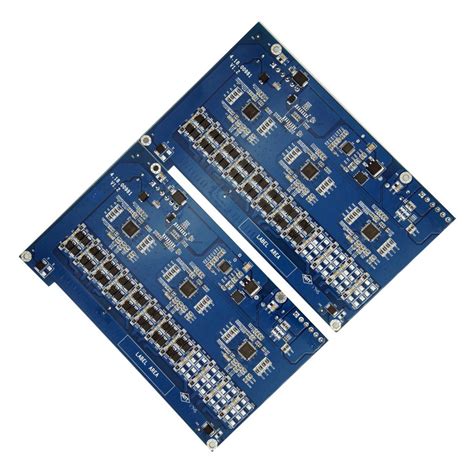
Collect the information on materials used for multilayer pcb
Understanding the Core Materials in Multilayer PCB Fabrication
In the realm of modern electronics, multilayer printed circuit boards (PCBs) have become indispensable due to their ability to support complex circuitry in a compact form. Understanding the core materials used in the fabrication of these multilayer PCBs is crucial for both designers and manufacturers aiming to optimize performance and reliability. The selection of materials not only influences the electrical properties but also affects the thermal and mechanical stability of the final product. Therefore, a comprehensive understanding of these materials is essential for anyone involved in PCB design and production.
At the heart of multilayer PCB fabrication lies the substrate material, which serves as the foundation for the entire board.
The most commonly used substrate is FR-4, a composite material made of woven fiberglass cloth with an epoxy resin binder that is flame resistant. FR-4 is favored for its excellent balance of cost, mechanical strength, and electrical insulation properties. However, as electronic devices become more sophisticated, the demand for substrates with superior performance characteristics has increased. Consequently, materials such as polyimide and PTFE (polytetrafluoroethylene) are gaining popularity. Polyimide offers high thermal stability and flexibility, making it suitable for applications that require bending or exposure to high temperatures. PTFE, on the other hand, is known for its low dielectric constant and loss, which are ideal for high-frequency applications.
In addition to the substrate, the copper foil used in multilayer PCBs is another critical component.
Copper is chosen for its excellent electrical conductivity, which is essential for efficient signal transmission. The thickness of the copper layer can vary depending on the specific requirements of the PCB, with common thicknesses ranging from 0.5 oz/ft² to 2 oz/ft². Thicker copper layers are often used in power electronics to handle higher current loads, while thinner layers are suitable for signal layers in high-density interconnects.
The dielectric materials used between the layers of copper are equally important.
These materials serve to insulate the conductive layers from each other while maintaining the board’s overall structural integrity. The choice of dielectric material can significantly impact the electrical performance of the PCB. For instance, materials with a low dielectric constant are preferred for high-speed digital and RF applications as they minimize signal loss and crosstalk. Common dielectric materials include epoxy resins, ceramics, and advanced composites, each offering distinct advantages depending on the application.
Furthermore, the solder mask, which is applied over the copper traces, plays a vital role in protecting the PCB from environmental factors such as moisture and dust.
It also prevents solder bridges during the assembly process. The solder mask is typically made from epoxy-based polymers, which provide a durable and heat-resistant coating.
Finally, the surface finish applied to the exposed copper areas is crucial for ensuring good solderability and protecting against oxidation. Common finishes include HASL (Hot Air Solder Leveling), ENIG (Electroless Nickel Immersion Gold), and OSP (Organic Solderability Preservative), each offering different benefits in terms of cost, reliability, and ease of assembly.
In conclusion, the materials used in multilayer PCB fabrication are diverse and selected based on a range of performance criteria. From the substrate and copper foil to the dielectric layers and surface finishes, each material plays a pivotal role in determining the functionality and durability of the final product. As technology continues to advance, the development of new materials will undoubtedly drive further innovation in PCB design and manufacturing.
The Role of Prepreg in Multilayer PCB Construction
In the realm of multilayer printed circuit boards (PCBs), the choice of materials plays a pivotal role in determining the performance, reliability, and overall functionality of the final product. Among these materials, prepreg stands out as a critical component in the construction of multilayer PCBs. Prepreg, short for pre-impregnated, refers to a composite material where a reinforcing fabric, typically fiberglass, is pre-impregnated with a resin system. This resin is partially cured, allowing the prepreg to remain flexible and tacky, which is essential for the lamination process in PCB manufacturing.
The primary function of prepreg in multilayer PCB construction is to act as an adhesive layer that bonds the various layers of the PCB together.
This bonding is crucial because it ensures the mechanical stability and integrity of the multilayer structure. As the number of layers in a PCB increases, the role of prepreg becomes even more significant, as it must provide consistent adhesion across all layers to prevent delamination and other structural failures. Furthermore, prepreg contributes to the dielectric properties of the PCB, influencing signal integrity and electrical performance.
Transitioning to the composition of prepreg, it is important to note that the resin system used in prepreg is typically an epoxy-based formulation.
Epoxy resins are favored due to their excellent mechanical properties, thermal stability, and electrical insulation characteristics. These properties are essential for maintaining the performance of the PCB under various environmental conditions, such as temperature fluctuations and mechanical stress. Additionally, the choice of fiberglass as the reinforcing fabric is due to its high tensile strength and low cost, making it an ideal material for mass production.
Moreover, the thickness and type of prepreg used can be tailored to meet specific design requirements.
For instance, different prepreg materials may be selected based on their dielectric constant, loss tangent, and thermal conductivity. These parameters are crucial for high-frequency applications, where signal integrity and thermal management are of paramount importance. By carefully selecting the appropriate prepreg material, designers can optimize the electrical performance of the PCB while ensuring its structural reliability.
In addition to its adhesive and dielectric functions, prepreg also plays a role in the thermal management of multilayer PCBs.
As electronic devices become more compact and powerful, the need for efficient heat dissipation becomes increasingly important. Prepreg materials with enhanced thermal conductivity can help dissipate heat away from critical components, thereby improving the overall thermal performance of the PCB. This is particularly relevant in applications such as telecommunications, automotive, and aerospace, where high power densities and harsh operating conditions are common.
In conclusion, prepreg is an indispensable material in the construction of multilayer PCBs, serving multiple functions that are crucial for the performance and reliability of the final product. Its role as an adhesive layer ensures the mechanical stability of the multilayer structure, while its dielectric properties influence the electrical performance of the PCB. Furthermore, the ability to tailor the properties of prepreg materials allows designers to meet specific design requirements, particularly in high-frequency and high-power applications. As technology continues to advance, the importance of selecting the right prepreg material will only grow, underscoring its vital role in the ever-evolving landscape of PCB manufacturing.
Copper Foil Types and Their Impact on Multilayer PCB Performance
In the realm of multilayer printed circuit boards (PCBs), the choice of materials plays a pivotal role in determining the overall performance and reliability of the final product. Among these materials, copper foil stands out as a critical component, influencing various aspects of the PCB’s functionality. Understanding the different types of copper foil and their impact on multilayer PCB performance is essential for engineers and designers aiming to optimize their designs.
Copper foil serves as the conductive layer in PCBs, facilitating the flow of electrical signals between components.
The two primary types of copper foil used in multilayer PCBs are electrodeposited (ED) copper foil and rolled annealed (RA) copper foil. Each type possesses distinct characteristics that affect the performance of the PCB in different ways.
Electrodeposited copper foil is produced through an electrochemical process, resulting in a foil with a columnar grain structure.
This type of copper foil is widely used due to its cost-effectiveness and ease of production. However, its columnar grain structure can lead to certain limitations, particularly in applications requiring high flexibility or thermal stability. Despite these limitations, ED copper foil is often preferred for applications where cost is a significant consideration and where the mechanical demands are not excessively stringent.
On the other hand, rolled annealed copper foil is manufactured through a mechanical rolling process, which produces a foil with a more uniform and dense grain structure.
This structure imparts superior mechanical properties, such as increased flexibility and better thermal performance, making RA copper foil an ideal choice for applications that demand high reliability and durability. The enhanced ductility of RA copper foil allows it to withstand repeated bending and flexing, which is particularly beneficial in flexible PCBs and applications subjected to dynamic mechanical stresses.
The choice between ED and RA copper foil can significantly impact the electrical performance of multilayer PCBs.
For instance, the smoother surface of RA copper foil can reduce signal loss and improve high-frequency performance, which is crucial in high-speed digital and RF applications. In contrast, the rougher surface of ED copper foil may introduce higher insertion loss, potentially affecting signal integrity in sensitive circuits.
Moreover, the thermal properties of the copper foil are also a critical consideration. RA copper foil, with its superior thermal conductivity, can enhance heat dissipation in multilayer PCBs, thereby improving the thermal management of the entire system. This is particularly important in high-power applications where efficient heat dissipation is necessary to prevent overheating and ensure long-term reliability.
In addition to the type of copper foil, the thickness of the foil is another factor that influences the performance of multilayer PCBs.
Thicker copper foils can carry higher currents and provide better heat dissipation, but they may also increase the overall weight and cost of the PCB. Therefore, selecting the appropriate copper foil thickness requires a careful balance between electrical, thermal, and mechanical requirements.
In conclusion, the choice of copper foil in multilayer PCBs is a critical decision that affects the electrical, thermal, and mechanical performance of the final product. By understanding the differences between electrodeposited and rolled annealed copper foils, as well as considering factors such as surface roughness and thickness, engineers can make informed decisions that optimize the performance and reliability of their multilayer PCB designs.
Dielectric Materials and Their Influence on Multilayer PCB Design
In the realm of multilayer printed circuit boards (PCBs), the choice of dielectric materials plays a pivotal role in determining the overall performance and reliability of the final product. As electronic devices become increasingly complex and compact, the demand for efficient multilayer PCBs has surged, necessitating a deeper understanding of the materials that constitute these intricate structures. Dielectric materials, which serve as insulators between conductive layers, are crucial in influencing the electrical properties, thermal management, and mechanical stability of multilayer PCBs.
To begin with, the primary function of dielectric materials in multilayer PCBs is to provide electrical insulation between the conductive copper layers.
This insulation is essential to prevent short circuits and ensure signal integrity. The dielectric constant, or permittivity, of these materials is a critical parameter that affects signal speed and impedance. Materials with a low dielectric constant are often preferred for high-frequency applications, as they allow signals to propagate faster and with less loss. Consequently, selecting the appropriate dielectric material is vital for optimizing the performance of high-speed and high-frequency circuits.
Moreover, the thermal properties of dielectric materials are equally important.
As electronic devices operate, they generate heat, which must be effectively dissipated to maintain functionality and prevent damage. Dielectric materials with high thermal conductivity are advantageous in facilitating heat dissipation, thereby enhancing the thermal management of the PCB. This is particularly crucial in multilayer designs, where heat can become trapped between layers, leading to potential overheating issues. Therefore, materials such as ceramic-filled polymers, which offer superior thermal conductivity, are often employed in multilayer PCB fabrication.
In addition to electrical and thermal considerations, the mechanical properties of dielectric materials also influence multilayer PCB design.
The material’s ability to withstand mechanical stress, such as bending and vibration, is essential for ensuring the durability and longevity of the PCB. Materials with high tensile strength and flexibility are preferred, as they can endure the rigors of manufacturing processes and operational environments. Furthermore, the coefficient of thermal expansion (CTE) of dielectric materials must be compatible with that of copper to prevent delamination and warping during thermal cycling.
Transitioning to the environmental and economic aspects, the choice of dielectric materials also impacts the sustainability and cost-effectiveness of multilayer PCBs.
With growing environmental concerns, there is an increasing emphasis on using materials that are not only efficient but also environmentally friendly. Halogen-free and lead-free materials are gaining popularity as they reduce the environmental footprint of electronic products. Additionally, the cost of dielectric materials can significantly influence the overall manufacturing expenses. Therefore, manufacturers must strike a balance between performance requirements and cost constraints when selecting materials for multilayer PCBs.
In conclusion, the selection of dielectric materials is a multifaceted decision that affects various aspects of multilayer PCB design, from electrical performance to thermal management and mechanical stability. As technology continues to advance, the development of innovative dielectric materials will be crucial in meeting the evolving demands of the electronics industry. By understanding the properties and implications of different dielectric materials, designers and manufacturers can optimize multilayer PCBs to achieve superior performance and reliability in a wide range of applications.