Ensuring Bare Copper Areas on PCB for Effective Tinning Processes
Key Takeaways
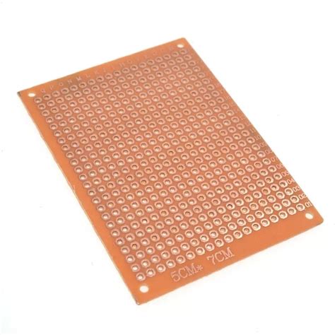
Ensuring adequate bare copper areas on your PCBs is essential for the overall effectiveness of the tinning process. By properly managing these regions, you can greatly enhance the adhesion of tin to copper surfaces, leading to a more reliable and durable finish. Start by considering methods for defining mask-free zones. This involves deciding which areas of your board require exposure during the PCB manufacturing process. Clearly delineating these regions allows you to maintain specific tracks and ground areas in their raw copper state, facilitating optimal tinning while minimizing potential issues.
Moreover, understanding how copper coverage impacts your design is crucial. It’s important to balance between sufficient coverage for electrical functionality and sufficient exposure for effective tinning. Check out the following table which summarizes best practices in managing copper areas:
| Best Practices | Description |
|---|---|
| Define Mask-Free Zones | Identify track and ground areas to remain exposed. |
| Monitor Copper Thickness | Ensure adequate copper thickness across the PCB. |
| Evaluate Tinning Materials | Choose materials that work well with bare copper. |
| Control PCB Manufacturing Cost | Optimize processes while maintaining quality standards. |
By adopting these strategies, you can effectively navigate challenges such as masking effects that may impede the efficiency of your tinning processes. Engaging with experienced PCB manufacturing companies can also provide insights into optimizing bare copper implementations in your designs, ensuring your business remains competitive while managing costs effectively in the ever-evolving landscape of PCB manufacturing.
Ensuring the Importance of Bare Copper Areas in PCB Tinning
When engaging in PCB manufacturing, understanding the significance of bare copper areas is paramount for successful tinning processes. These exposed copper surfaces facilitate a strong bond between the copper and tin, enhancing soldering capabilities. If you’re involved with PCB manufacturing companies, you’ll recognize that maintaining these areas during production directly impacts the final product’s reliability and performance. You must focus on defining mask-free zones that ensure these copper sections remain untouched throughout the etching and plating processes. This step is essential not only for achieving optimal PCB manufacturing cost efficiency but also for minimizing defects that can arise from inadequate surface preparation. By prioritizing bare copper zones in your designs, you effectively contribute to a smoother PCB manufacturing business operation, resulting in higher quality assemblies capable of meeting rigorous industry standards. Taking these aspects into account can significantly improve yield rates and customer satisfaction while reducing overall production times.
Methods for Defining Mask-Free Zones on PCBs
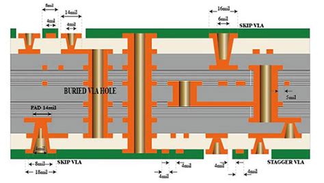
Defining mask-free zones on your PCB is pivotal for ensuring optimal results in the tinning process. One effective method is to start by identifying the areas that require exposure. This involves a thorough analysis of your design to highlight specific tracks and ground areas that must remain bare copper during processes. Utilize appropriate software tools during the PCB manufacturing stage to draw out these zones accurately, allowing you to strategically place your masking layers on the remaining sections. When working with PCB manufacturing companies, communicate your requirements clearly to ensure they comprehend where these mask-free zones are located within your design. Additionally, consider the implications of the PCB manufacturing cost—defining mask-free areas can sometimes lead to savings by reducing excess copper deposition and minimizing etching errors. Moreover, a well-planned approach not only aids in enhancing the aesthetics of your PCB but can also significantly boost its functionality and reliability for high-performance applications in your pcb manufacturing business. Thus, investing time in defining these zones will pay dividends through improved results and efficiency during subsequent production steps.
Techniques for Exposing Specific Tracks and Ground Areas
In the realm of PCB manufacturing, ensuring that specific tracks and ground areas are exposed is integral for effective tinning processes. One effective technique involves using a well-defined masking strategy that clearly delineates mask-free zones. These zones should be strategically designed so that necessary tracks, as well as the ground areas, remain unmasked during the PCB manufacturing process. As you work with PCB manufacturing companies, ensure you communicate your design intentions clearly; this clarity is vital to avoid any costly PCB manufacturing costs associated with rework or adjustments. Incorporating features such as design rules for exposed copper can further streamline this process. Moreover, utilizing software tools that allow for real-time visualization can help in verifying that your design adheres to the specifications needed for bare copper exposure. Remember, maintaining a balance between coverage and exposure in the PCB manufacturing business will ultimately enhance tinning efficiency, resulting in higher quality end products.
Best Practices for Managing Copper Coverage in PCB Design
When embarking on the intricate journey of PCB manufacturing, one of the pivotal aspects to consider is the management of copper coverage. Ensuring that bare copper areas are strategically allocated on your PCB is vital for achieving optimal results during the tinning processes. As you design your circuit boards, it’s essential to prioritize areas that need to remain exposed, particularly if you are working with PCB manufacturing companies that focus heavily on the efficiency of the soldering process.
To manage copper coverage effectively, you may employ techniques such as defining clear mask-free zones. This approach not only safeguards the specific tracks and ground areas but also minimizes unnecessary coverage that could complicate later manufacturing stages. Remember, maintaining a balance between aesthetics and functionality can influence your overall PCB manufacturing costs. By judiciously exposing specific regions, you ensure better adhesion during tinning, significantly enhancing the reliability of connections.
“A moment spent in planning saves great error,” – a wise reminder that underscores the value of meticulous design in your PCB manufacturing business. Regularly revisiting and refining your designs can lead to significant improvements in efficiency and product quality. Strive for continuous enhancement in managing bare copper areas; it could make all the difference in achieving excellence in PCB fabrication while mitigating potential costs related to rework or poor soldering outcomes.
Challenges and Solutions for Maintaining Bare Copper on PCBs
Maintaining bare copper areas on PCBs during the manufacturing process presents several challenges that can affect the overall efficiency and quality of your pcb manufacturing. One primary concern is ensuring that the copper remains free from any contaminants, which can lead to poor solderability and affect the effectiveness of subsequent tinning processes. You must be mindful of the environment in which your PCBs are produced, considering factors such as humidity and pollutants from nearby processes or materials. Another challenge arises from the techniques used to define mask-free zones during manufacturing. You should work closely with pcb manufacturing companies to choose approaches that accurately expose the desired tracks and ground areas without compromising other sections of the board.
Moreover, it’s essential to address the potential costs associated with maintaining these bare copper surfaces. The pcb manufacturing cost may rise if additional measures are necessary to protect these areas or rectify any issues stemming from mask placements or handling during fabrication. Collaborating with experienced partners in your pcb manufacturing business may provide insights and best practices for minimizing these costs without sacrificing quality.
Implementing specific strategies, such as using protective films that shield exposed copper while allowing for effective processing and ensuring adequate inspection protocols, can address these challenges. By being proactive in your design and process preparation, you can maintain quality bare copper areas while optimizing efficiency in your production line.
Evaluating the Impact of Masking on Tinning Efficiency
In the realm of PCB manufacturing, the way you mask bare copper areas can significantly influence the efficiency of tinning processes. When designing your printed circuit boards, it is crucial to consider how different masking techniques can either enhance or hinder the exposure of bare copper sections that are vital for effective tinning. Overly aggressive masking may lead to partial coverage or inconsistent solderability, which can ultimately affect the overall quality of your PCB manufacturing business. By identifying optimum mask-free zones, you allow essential tracks and ground areas to remain accessible for tinning, thereby improving your board’s performance and reliability. Additionally, a balanced approach ensures that your PCB manufacturing cost remains within budget while still meeting industry standards. It’s important to keep in mind that even slight alterations in your masking strategy can have profound repercussions on both long-term durability and immediate solder adhesion properties, shaping the success of your project within a competitive landscape filled with various PCB manufacturing companies.
Real-World Examples of Effective Bare Copper Implementations
In the realm of PCB manufacturing, several companies have successfully demonstrated innovative approaches to maintaining bare copper areas during the production process. For instance, a leading PCB manufacturing business utilized advanced imaging technology to precisely define mask-free zones, ensuring that the critical tracks and ground areas remained exposed while other elements were protected. This technique not only improved the effectiveness of tinning processes but also optimized overall production efficiency. Furthermore, by experimenting with different chemical formulations during the etching phase, these companies have managed to significantly reduce the PCB manufacturing cost, allowing for increased flexibility in design without sacrificing quality. Implementing these best practices has also provided measurable benefits in terms of electrical performance and longevity for the end products, illustrating how thoughtful management of bare copper areas can lead to advantageous outcomes in real-world applications. The positive results from these implementations highlight the importance of effective strategies for maintaining bare copper integrity, which is essential for enhancing operational efficiency and meeting customer demands in a competitive market among various PCB manufacturing companies.
Conclusion
In the realm of PCB manufacturing, understanding the significance of maintaining bare copper areas is crucial for the tinning processes to be effective. You should recognize that mask-free zones not only enhance the adhesion of solder but also significantly impact the overall performance of your PCB. By carefully defining these areas, you ensure that specific tracks and ground connections remain exposed during PCB manufacturing, allowing for superior electrical connectivity. It’s important to stay informed about the methods employed by leading PCB manufacturing companies when it comes to optimizing these bare copper sections, as this can directly affect your project’s outcome and its associated costs. Moreover, by adopting best practices in designing your PCB while being mindful of copper coverage, you can enhance both product reliability and efficiency, thereby improving your overall PCB manufacturing business performance. Keeping abreast of challenges in maintaining these bare copper regions and implementing solutions will ultimately contribute positively to your success in this competitive field.
FAQs
What is the significance of bare copper areas on PCBs?
Bare copper areas are crucial in PCB manufacturing as they facilitate proper tinning processes. Without adequately exposed copper, the solder may not adhere correctly, impacting the overall reliability of the circuit.
How can I ensure mask-free zones for effective tinning in PCB design?
To define mask-free zones, you should carefully plan your PCB manufacturing layout. This involves creating specific design rules that leave certain tracks and ground areas exposed, thereby ensuring they remain bare copper until the tinning process is completed.
What challenges might I face in managing bare copper on my PCBs?
One common challenge is oxidation, which can occur quickly on bare copper surfaces. Incorporating manufacturer recommendations from PCB manufacturing companies will help mitigate issues related to oxidation and ensure reliable performance in various environmental conditions.
What techniques are effective for exposing specific tracks and ground areas?
Utilizing design software that allows for precise control over pcb manufacturing cost will enable you to designate tracks and ground planes that should remain exposed. You might also consider using via-in-pad designs to assist with controlling exposure during the PCB production processes.
How does masking impact tinning efficiency during PCB production?
Improper masking can lead to either excessive or inadequate tinning, affecting solderability. To optimize results in your pcb manufacturing business, it’s imperative to assess the impact of your masking strategies on the overall effectiveness of tinning.
For further details on how to enhance your PCB manufacturing process, especially concerning bare copper areas and effective tinning, please click here: https://www.andwinpcb.com/pcb-manufacturing/

