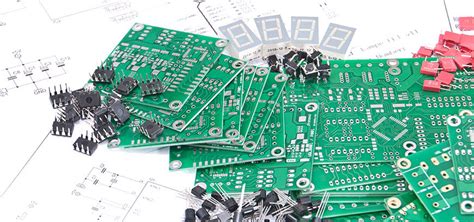
Copper clad pcb board
Advantages Of Using Copper Clad PCB Boards In Electronics
Copper clad PCB boards have become a cornerstone in the electronics industry, offering a multitude of advantages that make them indispensable in the design and manufacturing of electronic devices. These boards, characterized by a thin layer of copper laminated onto a non-conductive substrate, serve as the foundation for mounting and interconnecting electronic components. The benefits of using copper clad PCB boards are numerous, and they significantly enhance the performance, reliability, and efficiency of electronic systems.
One of the primary advantages of copper clad PCB boards is their excellent electrical conductivity.
Copper is renowned for its superior ability to conduct electricity, which ensures minimal energy loss during signal transmission. This high conductivity is crucial in maintaining the integrity of electrical signals, especially in high-frequency applications where signal degradation can lead to performance issues. Consequently, devices that utilize copper clad PCB boards often exhibit enhanced operational efficiency and reliability.
In addition to their electrical properties, copper clad PCB boards offer remarkable thermal management capabilities.
Electronic components generate heat during operation, and effective heat dissipation is essential to prevent overheating and potential damage. Copper’s high thermal conductivity allows it to efficiently transfer heat away from critical components, thereby maintaining optimal operating temperatures. This thermal management capability not only extends the lifespan of electronic devices but also enhances their performance by preventing thermal-induced failures.
Moreover, copper clad PCB boards are highly versatile, accommodating a wide range of design requirements.
They can be easily customized to fit specific applications, whether in consumer electronics, telecommunications, automotive systems, or industrial equipment. This adaptability is facilitated by the ability to etch intricate circuit patterns onto the copper layer, allowing for complex and compact designs. As a result, manufacturers can produce smaller, lighter, and more efficient electronic devices without compromising on functionality or performance.
Another significant advantage of copper clad PCB boards is their durability and mechanical strength.
The copper layer provides a robust surface that can withstand physical stress and environmental factors, such as moisture and temperature fluctuations. This durability ensures that the boards maintain their structural integrity over time, reducing the likelihood of mechanical failures. Additionally, the use of high-quality substrates further enhances the board’s resistance to wear and tear, making them suitable for use in demanding applications.
Furthermore, copper clad PCB boards contribute to cost-effectiveness in electronic manufacturing.
The efficiency of copper in conducting electricity and dissipating heat reduces the need for additional components, such as heat sinks or extra wiring, thereby lowering production costs. Additionally, the ability to produce complex circuits on a single board minimizes assembly time and labor costs. These factors, combined with the long-term reliability of copper clad PCB boards, result in significant cost savings for manufacturers and consumers alike.
In conclusion, the advantages of using copper clad PCB boards in electronics are manifold, encompassing superior electrical conductivity, effective thermal management, versatility in design, durability, and cost-effectiveness. These benefits make copper clad PCB boards an essential component in the development of modern electronic devices, ensuring that they meet the ever-increasing demands for performance, reliability, and efficiency. As technology continues to advance, the role of copper clad PCB boards in shaping the future of electronics remains pivotal, underscoring their enduring value in the industry.

Manufacturing Process Of Copper Clad PCB Boards
The manufacturing process of copper clad printed circuit boards (PCBs) is a meticulous and intricate procedure that plays a crucial role in the electronics industry. Copper clad PCBs serve as the foundational platform for mounting electronic components, and their quality directly impacts the performance and reliability of electronic devices. Understanding the manufacturing process of these boards is essential for appreciating their significance in modern technology.
To begin with, the process starts with the selection of the base material, typically a fiberglass-reinforced epoxy resin, known as FR-4.
This material is chosen for its excellent insulating properties and mechanical strength. The base material is then laminated with a thin layer of copper foil on one or both sides, creating what is known as a copper clad laminate. The thickness of the copper layer can vary depending on the specific requirements of the PCB, with common thicknesses ranging from 0.5 to 3 ounces per square foot.
Following the preparation of the copper clad laminate, the next step involves the application of a photosensitive resist layer.
This is achieved through a process called photolithography, where the resist is applied to the copper surface and then exposed to ultraviolet light through a photomask. The photomask contains the desired circuit pattern, and the exposure to UV light causes the resist to harden in the areas where the circuit paths are to be formed. Subsequently, the unhardened resist is removed, revealing the underlying copper that needs to be etched away.
The etching process is a critical phase in the manufacturing of copper clad PCBs.
It involves the use of chemical solutions, such as ferric chloride or ammonium persulfate, to dissolve the exposed copper, leaving behind the desired circuit pattern. This step requires precision and control to ensure that the etching is uniform and that the circuit paths are accurately defined. Once the etching is complete, the remaining resist is stripped away, exposing the copper circuit paths.
After the etching process, the PCB undergoes a series of cleaning and inspection steps to ensure that the circuit paths are free from defects and contaminants.
This is followed by the application of a solder mask, which is a protective layer that covers the entire surface of the PCB except for the areas where components will be soldered. The solder mask not only protects the copper traces from oxidation and environmental damage but also prevents solder bridges during the assembly process.
The final stages of manufacturing involve drilling holes for component leads and vias, which are plated through to establish electrical connections between different layers of the PCB. The board is then subjected to a surface finish process, such as hot air solder leveling or immersion gold plating, to enhance solderability and protect the exposed copper surfaces.
In conclusion, the manufacturing process of copper clad PCB boards is a complex and precise operation that requires careful attention to detail at every stage. From the selection of materials to the final surface finish, each step is crucial in ensuring the functionality and reliability of the finished product. As technology continues to advance, the demand for high-quality PCBs will only increase, underscoring the importance of understanding and optimizing their manufacturing processes.
Applications Of Copper Clad PCB Boards In Modern Technology
Copper clad PCB boards, integral components in the realm of modern electronics, have become indispensable due to their unique properties and versatile applications. These boards, characterized by a thin layer of copper laminated onto a non-conductive substrate, serve as the foundational building blocks for a myriad of electronic devices. Their significance in contemporary technology cannot be overstated, as they facilitate the efficient transmission of electrical signals, thereby enhancing the performance and reliability of electronic systems.
One of the primary applications of copper clad PCB boards is in consumer electronics, where they are used extensively in devices such as smartphones, tablets, and laptops.
The miniaturization of electronic components has necessitated the use of compact and efficient circuit boards, and copper clad PCBs meet these requirements with aplomb. Their ability to support high-density circuitry allows manufacturers to design smaller, more powerful devices that cater to the ever-growing demand for portable technology. Furthermore, the excellent thermal conductivity of copper helps in dissipating heat generated by electronic components, thereby prolonging the lifespan of these devices.
In addition to consumer electronics, copper clad PCB boards play a crucial role in the automotive industry.
Modern vehicles are equipped with a plethora of electronic systems, ranging from engine control units to advanced driver-assistance systems. These systems rely heavily on the robust performance of copper clad PCBs to ensure seamless operation. The boards’ durability and resistance to environmental factors such as temperature fluctuations and vibrations make them ideal for automotive applications. As the industry moves towards electric and autonomous vehicles, the demand for reliable and efficient PCB boards is expected to rise, further cementing their importance in automotive technology.
The telecommunications sector also benefits significantly from the use of copper clad PCB boards.
With the advent of 5G technology and the increasing need for high-speed data transmission, the role of PCBs in telecommunications infrastructure has become more critical than ever. Copper clad boards are used in the construction of base stations, routers, and other communication devices, where they facilitate the rapid and reliable transmission of data. Their ability to support high-frequency signals without significant loss makes them indispensable in maintaining the integrity and efficiency of communication networks.
Moreover, copper clad PCB boards are pivotal in the medical field, where precision and reliability are paramount.
Medical devices such as MRI machines, pacemakers, and diagnostic equipment rely on these boards to function accurately and consistently. The boards’ ability to handle complex circuitry and their resistance to interference ensure that medical devices operate without fail, thereby safeguarding patient health and well-being. As medical technology continues to advance, the demand for sophisticated PCB solutions is likely to grow, highlighting the ongoing relevance of copper clad boards in this sector.
In conclusion, the applications of copper clad PCB boards in modern technology are vast and varied, spanning industries such as consumer electronics, automotive, telecommunications, and healthcare.
Their unique properties, including excellent thermal conductivity, durability, and the ability to support high-density and high-frequency circuits, make them indispensable in the development and functioning of contemporary electronic systems. As technology continues to evolve, the role of copper clad PCB boards is expected to expand further, underscoring their critical importance in shaping the future of modern technology.
Comparing Copper Clad PCB Boards To Other PCB Types
Copper clad PCB boards, a fundamental component in the electronics industry, are often compared to other types of printed circuit boards (PCBs) due to their unique properties and applications. Understanding the distinctions between copper clad PCBs and other PCB types is crucial for selecting the appropriate board for specific electronic applications.
Copper clad PCBs are characterized by a thin layer of copper laminated onto a non-conductive substrate.
This copper layer serves as the conductive path for electrical signals, making these boards essential in the creation of electronic circuits. The primary advantage of copper clad PCBs lies in their excellent conductivity, which ensures efficient signal transmission and minimal energy loss. This feature is particularly beneficial in high-frequency applications where signal integrity is paramount.
In contrast, other PCB types, such as aluminum-based PCBs, offer different advantages.
Aluminum PCBs are known for their superior heat dissipation properties, making them ideal for applications involving high power and heat generation, such as LED lighting and power converters. While copper clad PCBs can also handle significant thermal loads, aluminum PCBs provide a more efficient solution for managing heat, thereby enhancing the longevity and reliability of electronic components.
Another type of PCB that warrants comparison is the flexible PCB.
Unlike the rigid structure of copper clad boards, flexible PCBs are designed to bend and conform to various shapes. This flexibility allows for innovative design solutions in compact and dynamic electronic devices, such as wearable technology and foldable smartphones. However, flexible PCBs may not offer the same level of conductivity as copper clad boards, which can be a limiting factor in applications requiring high-speed data transmission.
Furthermore, multilayer PCBs present another alternative, offering the ability to incorporate multiple layers of copper and substrate materials.
This design allows for complex circuit configurations and increased functionality within a compact space. While copper clad PCBs can be manufactured as single or double-sided boards, multilayer PCBs provide a more versatile solution for intricate electronic systems. However, the complexity and cost of manufacturing multilayer PCBs can be significantly higher compared to simpler copper clad designs.
When considering the environmental impact, copper clad PCBs have an edge due to their recyclability.
The copper used in these boards can be reclaimed and reused, reducing waste and promoting sustainability. In contrast, some other PCB types, particularly those involving composite materials or specialized coatings, may pose greater challenges in terms of recycling and environmental impact.
In conclusion, the choice between copper clad PCBs and other PCB types depends largely on the specific requirements of the application.
Copper clad PCBs offer excellent conductivity and are well-suited for applications where signal integrity is critical. However, for applications requiring superior heat management, flexibility, or complex circuit designs, other PCB types such as aluminum, flexible, or multilayer boards may be more appropriate. By carefully evaluating the unique properties and advantages of each PCB type, engineers and designers can make informed decisions that optimize performance, cost, and sustainability in their electronic projects.
Environmental Impact And Recycling Of Copper Clad PCB Boards
Copper clad printed circuit boards (PCBs) are integral components in modern electronic devices, serving as the backbone for electrical connectivity. However, as the demand for electronic devices continues to surge, the environmental impact of these boards has become a growing concern. Understanding the environmental implications and exploring recycling options for copper clad PCBs is crucial for sustainable development.
The production of copper clad PCBs involves several processes that can have significant environmental consequences.
Initially, the extraction and processing of copper, a key material in these boards, contribute to environmental degradation. Mining activities often lead to habitat destruction, soil erosion, and water pollution. Furthermore, the energy-intensive nature of copper processing results in substantial greenhouse gas emissions. As a result, the environmental footprint of copper production is considerable, necessitating a shift towards more sustainable practices.
In addition to the environmental impact of copper extraction, the manufacturing process of PCBs involves the use of various chemicals and materials that can be harmful to the environment.
For instance, the etching process, which removes excess copper to create circuit patterns, often employs hazardous chemicals such as ferric chloride. These chemicals, if not properly managed, can lead to soil and water contamination. Moreover, the lamination process, which bonds copper layers to a substrate, typically uses epoxy resins that are not biodegradable, further exacerbating the environmental challenges associated with PCB production.
Given these environmental concerns, recycling copper clad PCBs has emerged as a viable solution to mitigate their impact.
Recycling not only conserves natural resources by recovering valuable materials but also reduces the need for new raw materials, thereby decreasing the environmental burden of mining and processing. The recycling process typically involves the collection and dismantling of electronic waste, followed by the separation of copper and other metals from non-metallic components. Advanced techniques such as hydrometallurgical and pyrometallurgical processes are employed to extract copper efficiently, ensuring minimal environmental harm.
Moreover, recycling copper clad PCBs can significantly reduce electronic waste, which is one of the fastest-growing waste streams globally
.By diverting these boards from landfills, recycling helps prevent the leaching of toxic substances into the environment. This is particularly important as PCBs often contain hazardous elements such as lead and mercury, which can pose serious health risks if not properly managed. Consequently, recycling not only addresses environmental concerns but also contributes to public health and safety.
Despite the clear benefits of recycling, several challenges remain.
The complexity of PCB design, with multiple layers and diverse materials, makes the recycling process technically demanding and costly. Additionally, the lack of standardized recycling practices and inadequate infrastructure in many regions hinders the widespread adoption of PCB recycling. To overcome these challenges, concerted efforts are needed from governments, industries, and consumers to promote recycling initiatives and invest in research and development for more efficient recycling technologies.
In conclusion, while copper clad PCBs are indispensable in the modern technological landscape, their environmental impact cannot be overlooked. By prioritizing recycling and sustainable practices, it is possible to mitigate the adverse effects associated with their production and disposal. Through collaborative efforts and innovative solutions, the electronics industry can move towards a more sustainable future, balancing technological advancement with environmental stewardship.