Custom flex pcb
Advantages Of Custom Flex PCB In Modern Electronics
Custom flexible printed circuit boards (PCBs) have emerged as a pivotal innovation in the realm of modern electronics, offering a multitude of advantages that cater to the evolving demands of contemporary technology. As electronic devices become increasingly compact and sophisticated, the need for adaptable and efficient circuit solutions has never been more pronounced. Custom flex PCBs, with their unique properties, address these needs by providing unparalleled flexibility, durability, and design versatility.
One of the foremost advantages of custom flex PCBs is their inherent flexibility, which allows them to be bent, folded, or twisted without compromising their functionality.
This characteristic is particularly beneficial in applications where space is at a premium, such as in wearable technology, medical devices, and compact consumer electronics. By enabling circuits to conform to the contours of a device, custom flex PCBs facilitate the creation of smaller, lighter, and more ergonomic products. This adaptability not only enhances the aesthetic appeal of electronic devices but also contributes to their overall performance by optimizing space utilization.
In addition to their flexibility, custom flex PCBs are renowned for their durability.
Constructed from robust materials such as polyimide or polyester, these PCBs are designed to withstand harsh environmental conditions, including extreme temperatures, moisture, and mechanical stress. This resilience makes them ideal for use in demanding applications, such as automotive and aerospace industries, where reliability and longevity are paramount. Furthermore, the ability of flex PCBs to absorb vibrations and shocks enhances the durability of the entire electronic assembly, reducing the risk of failure and extending the lifespan of the device.
Another significant advantage of custom flex PCBs is their design versatility.
Unlike traditional rigid PCBs, which are limited by their fixed shape and size, flex PCBs can be tailored to meet specific design requirements. This customization extends to the layout, shape, and thickness of the circuit, allowing engineers to create innovative solutions that align with the unique needs of their projects. The ability to integrate multiple components and functions into a single flex PCB also simplifies the assembly process, reducing the number of interconnections and potential points of failure. Consequently, this leads to improved signal integrity and enhanced overall performance of the electronic device.
Moreover, custom flex PCBs contribute to cost efficiency in the manufacturing process.
By minimizing the need for additional connectors and cables, these PCBs reduce material costs and assembly time. The streamlined design also facilitates easier testing and troubleshooting, further lowering production expenses. As a result, manufacturers can achieve significant cost savings while maintaining high-quality standards, making custom flex PCBs an economically viable option for a wide range of applications.
In conclusion, the advantages of custom flex PCBs in modern electronics are manifold, encompassing flexibility, durability, design versatility, and cost efficiency.
As technology continues to advance, the demand for innovative circuit solutions that can accommodate the complexities of modern devices will only increase. Custom flex PCBs, with their ability to adapt to diverse requirements and withstand challenging conditions, are poised to play an integral role in shaping the future of electronic design and manufacturing. By embracing these cutting-edge solutions, industries can unlock new possibilities and drive the development of next-generation technologies.

Design Considerations For Custom Flex PCB
When embarking on the design of custom flexible printed circuit boards (PCBs), several critical considerations must be taken into account to ensure optimal performance and reliability. Custom flex PCBs offer unique advantages, such as the ability to fit into compact spaces and endure dynamic flexing, making them ideal for a wide range of applications, from consumer electronics to medical devices. However, the design process for these versatile components requires meticulous attention to detail and a comprehensive understanding of the factors that influence their functionality.
To begin with, material selection is paramount in the design of custom flex PCBs.
The choice of substrate material, typically polyimide, is crucial due to its excellent thermal stability and flexibility. Polyimide’s ability to withstand high temperatures and its inherent flexibility make it a preferred choice for applications that demand durability and resilience.
Additionally, the copper foil used in the circuit must be carefully selected to balance conductivity with flexibility.
Thinner copper layers are often preferred to enhance the board’s ability to bend without compromising electrical performance.
Transitioning from material considerations, the layout design of a custom flex PCB is another critical aspect.
The layout must be meticulously planned to accommodate the unique mechanical and electrical requirements of the application. Designers must consider the bend radius, which is the minimum radius the flex PCB can be bent without causing damage. A larger bend radius is generally recommended to prevent stress on the copper traces and substrate, thereby enhancing the board’s longevity. Furthermore, trace routing should be optimized to minimize stress concentration, with traces ideally running perpendicular to the bend lines to reduce the risk of cracking.
In addition to layout considerations, the choice of adhesive and coverlay materials plays a significant role in the design of custom flex PCBs.
Adhesives are used to bond the layers of the PCB, and their selection must ensure compatibility with the substrate and copper materials. The coverlay, which protects the circuit from environmental factors and mechanical damage, must be flexible enough to accommodate the board’s bending requirements while providing adequate protection. The thickness and material of the coverlay should be chosen based on the specific environmental conditions the PCB will encounter.
Moreover, the design process must also account for the manufacturing capabilities and limitations.
It is essential to collaborate closely with the PCB manufacturer to ensure that the design can be effectively translated into a physical product. This collaboration helps in understanding the tolerances and constraints of the manufacturing process, such as minimum trace widths and spacing, which can significantly impact the final product’s performance and reliability.
Finally, testing and validation are indispensable components of the design process for custom flex PCBs.
Rigorous testing under simulated operating conditions is necessary to verify that the PCB meets all performance and reliability requirements. This includes testing for electrical continuity, insulation resistance, and mechanical durability. By thoroughly validating the design, potential issues can be identified and addressed before mass production, thereby reducing the risk of failure in the field.
In conclusion, designing custom flex PCBs involves a complex interplay of material selection, layout design, adhesive and coverlay choices, manufacturing considerations, and thorough testing. By carefully addressing each of these factors, designers can create flexible PCBs that meet the demanding requirements of modern applications, ensuring both performance and reliability in their intended use.
Manufacturing Process Of Custom Flex PCB
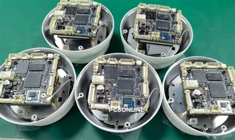
The manufacturing process of custom flex printed circuit boards (PCBs) is a sophisticated and intricate procedure that requires precision and expertise. Flex PCBs, known for their flexibility and ability to fit into compact spaces, are increasingly in demand across various industries, including consumer electronics, automotive, and medical devices. Understanding the manufacturing process of these custom flex PCBs is crucial for ensuring their reliability and performance in critical applications.
To begin with, the process starts with the design phase, where engineers create a detailed blueprint of the circuit layout.
This design is crucial as it dictates the functionality and efficiency of the final product. Advanced software tools are employed to simulate and optimize the design, ensuring that it meets the specific requirements of the application. Once the design is finalized, it is converted into a format suitable for manufacturing, typically a Gerber file, which contains all the necessary information for the production process.
Following the design phase, the next step is the selection of materials.
Flex PCBs are typically made from a flexible substrate, such as polyimide, which provides the necessary flexibility and thermal stability. The choice of materials is critical, as it affects the board’s performance, durability, and cost. Conductive materials, usually copper, are then laminated onto the substrate to form the circuit traces. This lamination process must be executed with precision to ensure that the conductive layers adhere properly to the substrate without any defects.
Subsequently, the manufacturing process moves to the etching stage, where unwanted copper is removed to reveal the desired circuit pattern.
This is achieved through a chemical etching process, which involves applying a photoresist to the copper layer, exposing it to ultraviolet light through a mask of the circuit pattern, and then developing it to remove the unexposed areas. The exposed copper is then etched away, leaving behind the precise circuit traces. This step requires meticulous attention to detail to prevent any over-etching or under-etching, which could compromise the circuit’s integrity.
After etching, the next phase involves drilling and plating.
Holes are drilled into the board to create vias, which allow for electrical connections between different layers of the PCB. These holes are then plated with copper to ensure conductivity. The plating process is critical, as it ensures that the electrical connections are robust and reliable. Any defects in this stage could lead to circuit failures, which are unacceptable in high-stakes applications.
Once the drilling and plating are complete, the board undergoes a series of inspections and tests to verify its quality and functionality.
These tests include electrical testing to ensure that the circuit operates as intended and visual inspections to check for any physical defects. Quality control is paramount in the manufacturing of custom flex PCBs, as even minor defects can lead to significant issues in the final application.
Finally, the flex PCB is cut to its final shape and size, and any additional components are assembled onto the board.
This assembly process may involve surface mounting or through-hole technology, depending on the design specifications. The completed PCB is then subjected to a final round of testing to ensure that it meets all the required standards and specifications.
In conclusion, the manufacturing process of custom flex PCBs is a complex and detailed procedure that demands precision at every stage. From design and material selection to etching, drilling, and assembly, each step is critical to producing a high-quality product that meets the specific needs of its application. As technology continues to advance, the demand for custom flex PCBs is expected to grow, making the understanding of their manufacturing process increasingly important.
Applications Of Custom Flex PCB In Various Industries
Custom flexible printed circuit boards (PCBs) have emerged as a pivotal innovation in the electronics industry, offering a myriad of applications across various sectors. These versatile components are designed to meet the specific needs of different industries, providing unique advantages that rigid PCBs cannot offer.
As technology continues to advance, the demand for custom flex PCBs is expected to grow, driven by their ability to enhance performance, reduce weight, and improve reliability in complex electronic systems.
One of the primary industries benefiting from custom flex PCBs is the consumer electronics sector.
In this fast-paced market, manufacturers are constantly seeking ways to create smaller, lighter, and more efficient devices. Custom flex PCBs are ideal for this purpose, as they can be designed to fit into compact spaces and conform to the intricate shapes of modern gadgets. Smartphones, tablets, and wearable devices, for instance, often incorporate these flexible circuits to accommodate their sleek designs and multifunctional capabilities. The flexibility of these PCBs allows for innovative product designs that were previously unattainable with traditional rigid boards.
In addition to consumer electronics, the automotive industry has also embraced custom flex PCBs.
As vehicles become increasingly sophisticated, with advanced infotainment systems, navigation aids, and safety features, the need for reliable and adaptable electronic components has grown. Custom flex PCBs are used in various automotive applications, including dashboard displays, engine management systems, and advanced driver-assistance systems (ADAS).
Their ability to withstand harsh environmental conditions, such as extreme temperatures and vibrations, makes them particularly suitable for automotive use.
Moreover, the lightweight nature of flex PCBs contributes to overall vehicle weight reduction, which is crucial for improving fuel efficiency and reducing emissions.
The medical industry is another sector where custom flex PCBs have made significant inroads.
Medical devices often require compact and reliable electronic components to function effectively. Custom flex PCBs are used in a wide range of medical applications, from diagnostic equipment to implantable devices. Their flexibility and biocompatibility make them ideal for use in devices that need to conform to the human body, such as pacemakers and hearing aids. Furthermore, the ability to customize these PCBs ensures that they meet the stringent regulatory standards required in the medical field, ensuring patient safety and device efficacy.
In the aerospace and defense industries, custom flex PCBs are valued for their durability and performance under extreme conditions.
These sectors demand electronic components that can operate reliably in high-stress environments, such as outer space or combat zones. Custom flex PCBs are used in satellite systems, avionics, and military communication devices, where their lightweight and flexible nature is advantageous. The ability to design these PCBs to meet specific requirements ensures that they can withstand the rigors of aerospace and defense applications, providing reliable performance in critical situations.
As we look to the future, the role of custom flex PCBs in various industries is set to expand further.
With the ongoing development of technologies such as the Internet of Things (IoT) and 5G, the demand for flexible, high-performance electronic components will continue to rise. Custom flex PCBs, with their adaptability and efficiency, are well-positioned to meet these emerging needs, driving innovation and enabling new possibilities across a wide range of applications. In conclusion, the versatility and advantages of custom flex PCBs make them an indispensable component in the modern technological landscape, with their applications spanning numerous industries and contributing to the advancement of electronic systems worldwide.