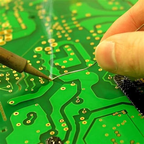
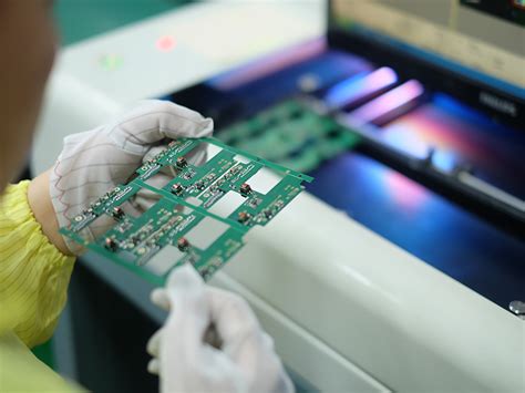
Digital high speed pcb application
Optimizing Signal Integrity in High-Speed PCB Design
In the realm of modern electronics, the demand for high-speed digital applications has surged, necessitating the development of printed circuit boards (PCBs) that can support these advanced technologies. As digital signals traverse these high-speed PCBs, maintaining signal integrity becomes paramount. Signal integrity refers to the preservation of the quality and fidelity of electrical signals as they travel through the PCB, ensuring that they reach their destination without distortion or loss. To optimize signal integrity in high-speed PCB design, engineers must consider a multitude of factors, each playing a crucial role in the overall performance of the circuit.
One of the primary considerations in optimizing signal integrity is the careful management of impedance.
Impedance mismatches can lead to signal reflections, which degrade the quality of the signal. To mitigate this, designers must ensure that the characteristic impedance of the transmission lines on the PCB is consistent and matches the impedance of the connected components. This involves precise control over the width and spacing of the traces, as well as the dielectric properties of the materials used in the PCB substrate. By maintaining a uniform impedance, signal reflections can be minimized, thereby preserving signal integrity.
In addition to impedance control, minimizing crosstalk is another critical aspect of high-speed PCB design.
Crosstalk occurs when signals in adjacent traces interfere with each other, leading to unwanted noise and potential data corruption. To reduce crosstalk, designers can employ techniques such as increasing the spacing between traces, using differential signaling, and incorporating ground planes. Ground planes, in particular, provide a low-impedance return path for signals, which helps to isolate them from one another and reduce electromagnetic interference.
Furthermore, the layout of the PCB plays a significant role in signal integrity.
A well-thought-out layout can significantly reduce the risk of signal degradation. For instance, keeping high-speed signal traces as short as possible minimizes the potential for signal loss and distortion. Additionally, avoiding sharp bends in traces and using smooth, gradual curves can prevent impedance discontinuities that may lead to signal reflections. The strategic placement of components is also essential, as it can help to minimize the length of critical signal paths and reduce the potential for interference.
Another important consideration is the power distribution network (PDN) within the PCB.
A stable and efficient PDN is crucial for maintaining signal integrity, as fluctuations in power can introduce noise into the system. To optimize the PDN, designers can use decoupling capacitors to filter out high-frequency noise and ensure a stable power supply to all components. Additionally, employing a multi-layer PCB design with dedicated power and ground planes can further enhance the stability of the power distribution network.
As technology continues to advance, the challenges associated with high-speed PCB design will only become more complex.
However, by focusing on key aspects such as impedance control, crosstalk reduction, layout optimization, and power distribution, engineers can effectively optimize signal integrity in high-speed digital applications. Through meticulous design and careful consideration of these factors, it is possible to create PCBs that not only meet the demands of modern technology but also ensure reliable and efficient performance. In conclusion, the pursuit of signal integrity in high-speed PCB design is a multifaceted endeavor that requires a comprehensive understanding of both the theoretical and practical aspects of electronics engineering.
Advanced Materials for High-Speed Digital PCBs
In the realm of high-speed digital printed circuit boards (PCBs), the selection of materials plays a pivotal role in determining the performance and reliability of the final product. As digital applications continue to demand faster data rates and higher frequencies, the need for advanced materials that can support these requirements has become increasingly critical. The choice of substrate materials, in particular, is a key factor that influences signal integrity, thermal management, and overall system performance.
To begin with, the dielectric constant (Dk) and dissipation factor (Df) of the substrate material are crucial parameters that affect signal propagation speed and loss.
Materials with a low dielectric constant are preferred for high-speed applications as they allow signals to travel faster, thereby reducing latency. Similarly, a low dissipation factor is essential to minimize signal loss, which is particularly important at higher frequencies where losses can be more pronounced. Advanced materials such as polytetrafluoroethylene (PTFE) composites and ceramic-filled laminates are often employed in high-speed digital PCBs due to their favorable dielectric properties.
Moreover, the thermal management capabilities of the substrate material cannot be overlooked.
As data rates increase, so does the power consumption and heat generation within the PCB. Efficient heat dissipation is necessary to prevent thermal-induced failures and ensure the longevity of the board. Materials with high thermal conductivity, such as metal-backed laminates or those with embedded heat spreaders, are increasingly being utilized to address these challenges. These materials help in maintaining optimal operating temperatures, thereby enhancing the reliability of high-speed digital applications.
In addition to dielectric and thermal properties, the mechanical stability of the substrate material is also a significant consideration.
High-speed digital PCBs often undergo various environmental stresses, including temperature fluctuations and mechanical vibrations. Therefore, materials that offer robust mechanical properties, such as high tensile strength and low thermal expansion, are essential to maintain structural integrity and prevent warping or delamination. Advanced composites and reinforced laminates are examples of materials that provide the necessary mechanical resilience for demanding applications.
Furthermore, as the industry moves towards miniaturization and higher component densities, the need for materials that support fine line etching and high layer counts becomes apparent. Advanced materials with smooth surface finishes and excellent dimensional stability are crucial for achieving the precision required in modern high-speed digital PCBs. These materials facilitate the fabrication of intricate circuit patterns and multilayer structures, which are essential for accommodating the complex routing and interconnections in high-speed designs.
In conclusion, the selection of advanced materials for high-speed digital PCBs is a multifaceted decision that impacts various aspects of performance and reliability.
By carefully considering the dielectric, thermal, mechanical, and fabrication properties of substrate materials, designers can optimize their PCB designs to meet the stringent demands of modern digital applications. As technology continues to evolve, the development and adoption of innovative materials will remain a cornerstone in advancing the capabilities of high-speed digital PCBs, ensuring they can keep pace with the ever-increasing demands of the digital age.
Thermal Management Techniques for High-Speed PCB Applications
In the realm of digital high-speed printed circuit board (PCB) applications, thermal management emerges as a critical consideration, ensuring both the reliability and performance of electronic devices. As the demand for faster processing speeds and higher power densities continues to rise, effective thermal management techniques become indispensable. The intricate design of high-speed PCBs, characterized by densely packed components and complex interconnections, necessitates innovative approaches to dissipate heat efficiently. Consequently, understanding and implementing these techniques is paramount for engineers and designers striving to optimize the functionality and longevity of electronic systems.
To begin with, one of the fundamental strategies in thermal management is the use of thermal vias.
These are strategically placed conductive pathways that facilitate the transfer of heat from the surface of the PCB to the inner layers or to an external heat sink. By providing a direct route for heat dissipation, thermal vias help in maintaining the temperature of critical components within safe operating limits. Moreover, the integration of thermal vias can be optimized by varying their size, number, and placement, thereby enhancing their effectiveness in heat management.
In addition to thermal vias, the selection of appropriate materials plays a pivotal role in thermal management.
High thermal conductivity materials, such as copper and aluminum, are often employed in the construction of PCBs to improve heat dissipation. These materials not only aid in the efficient transfer of heat but also contribute to the overall structural integrity of the board. Furthermore, the use of thermal interface materials (TIMs) between components and heat sinks can significantly reduce thermal resistance, ensuring a more uniform temperature distribution across the PCB.
Another crucial aspect of thermal management in high-speed PCB applications is the design of heat sinks.
These components are specifically engineered to absorb and dissipate heat away from critical areas of the PCB. By increasing the surface area available for heat exchange, heat sinks facilitate the efficient transfer of thermal energy to the surrounding environment. The design of heat sinks can be tailored to meet specific requirements, with variations in size, shape, and material composition allowing for customized solutions that address the unique thermal challenges of each application.
Moreover, active cooling methods, such as the use of fans or liquid cooling systems, can be employed to enhance thermal management in high-speed PCBs
. While passive cooling techniques rely on natural convection and conduction, active cooling introduces forced convection, thereby increasing the rate of heat dissipation. Although these methods may involve additional complexity and cost, they offer significant advantages in applications where passive cooling alone is insufficient to maintain optimal operating temperatures.
In conclusion, the effective management of thermal energy in digital high-speed PCB applications is a multifaceted challenge that requires a comprehensive understanding of various techniques and materials. By employing a combination of thermal vias, high-conductivity materials, heat sinks, and active cooling methods, engineers can ensure that electronic devices operate efficiently and reliably. As technology continues to advance, the importance of innovative thermal management solutions will only grow, underscoring the need for ongoing research and development in this critical area. Through meticulous design and strategic implementation, the thermal challenges associated with high-speed PCBs can be successfully addressed, paving the way for the next generation of electronic innovations.
Design Considerations for High-Speed Digital PCB Layout
In the realm of modern electronics, the demand for high-speed digital circuits has surged, necessitating meticulous attention to the design of printed circuit boards (PCBs). High-speed digital PCB layout is a critical aspect that influences the performance, reliability, and functionality of electronic devices. As digital signals traverse the PCB at increasingly higher speeds, designers must consider a multitude of factors to ensure signal integrity and minimize potential issues such as electromagnetic interference (EMI) and crosstalk.
To begin with, one of the primary considerations in high-speed digital PCB design is the management of signal integrity.
Signal integrity refers to the preservation of the quality of electrical signals as they propagate through the PCB. High-speed signals are susceptible to distortion, which can lead to data errors and system malfunctions. To mitigate these risks, designers must carefully plan the trace layout, ensuring that traces are as short and direct as possible. Additionally, maintaining consistent trace impedance is crucial, as impedance mismatches can cause signal reflections and degrade signal quality.
Moreover, the choice of materials plays a pivotal role in high-speed PCB design.
The dielectric constant and loss tangent of the substrate material can significantly impact signal propagation. Low-loss materials are preferred for high-speed applications as they reduce signal attenuation and maintain signal integrity over longer distances. Furthermore, the use of advanced materials can help in managing thermal performance, which is another critical aspect of high-speed PCB design. As components operate at higher speeds, they tend to generate more heat, necessitating effective thermal management strategies to prevent overheating and ensure reliable operation.
Transitioning to another vital consideration, the power distribution network (PDN) must be meticulously designed to provide stable and clean power to all components.
High-speed circuits are particularly sensitive to power fluctuations, which can introduce noise and affect performance. To address this, designers often employ techniques such as decoupling capacitors and power planes to minimize voltage fluctuations and ensure a robust PDN. Additionally, careful placement of components and strategic routing of power traces can further enhance power integrity.
In addition to these considerations, managing electromagnetic interference (EMI) is paramount in high-speed digital PCB design.
EMI can emanate from various sources, including high-frequency signals and switching power supplies, potentially affecting the performance of nearby circuits. To mitigate EMI, designers can implement shielding techniques, such as ground planes and guard traces, to isolate sensitive signals. Moreover, maintaining proper spacing between traces and employing differential signaling can help reduce EMI and crosstalk, ensuring that signals remain clean and undistorted.
Finally, the integration of simulation tools into the design process is indispensable for high-speed digital PCB layout.
Simulation allows designers to model and analyze the behavior of high-speed signals, identify potential issues, and optimize the design before physical prototyping. By leveraging simulation, designers can predict the impact of various design choices on signal integrity, EMI, and thermal performance, ultimately leading to more robust and reliable PCB designs.
In conclusion, designing high-speed digital PCBs requires a comprehensive understanding of various factors that influence signal integrity, power distribution, EMI, and thermal management. By carefully considering these aspects and employing advanced materials and simulation tools, designers can create PCBs that meet the demands of modern high-speed digital applications, ensuring optimal performance and reliability in an increasingly connected world.