Flex pcb cable
Advantages Of Using Flex PCB Cables In Modern Electronics
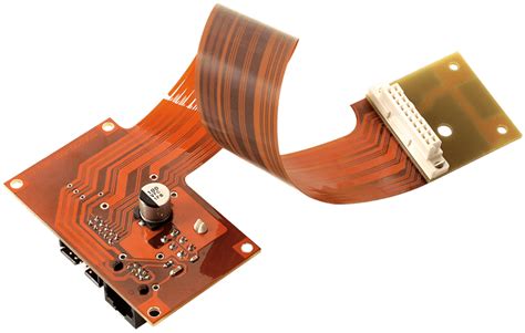
Flex PCB cables, or flexible printed circuit board cables, have become an integral component in the design and functionality of modern electronic devices. Their unique properties and advantages over traditional rigid PCBs make them an attractive choice for engineers and designers seeking to innovate and optimize electronic products.
One of the primary advantages of flex PCB cables is their ability to conform to complex shapes and fit into tight spaces.
This flexibility allows for more compact and lightweight designs, which is particularly beneficial in the development of portable and wearable electronics. As devices continue to shrink in size, the demand for components that can adapt to these constraints without compromising performance has increased, making flex PCB cables an ideal solution.
In addition to their adaptability, flex PCB cables offer enhanced durability and reliability.
The materials used in their construction, such as polyimide or polyester films, provide excellent resistance to environmental factors like heat, moisture, and chemicals. This resilience ensures that the cables maintain their integrity and functionality even in harsh conditions, which is crucial for applications in industries such as automotive, aerospace, and medical devices. Furthermore, the reduced number of connectors and solder joints in flex PCB designs minimizes potential points of failure, thereby increasing the overall reliability of the electronic system.
Another significant advantage of flex PCB cables is their ability to reduce electromagnetic interference (EMI).
The design of these cables allows for better control of the electromagnetic fields, which can be particularly important in high-frequency applications. By minimizing EMI, flex PCB cables help ensure the proper functioning of sensitive electronic components and improve the overall performance of the device. This characteristic is especially valuable in communication devices and other electronics where signal integrity is paramount.
Moreover, flex PCB cables contribute to cost savings in both manufacturing and assembly processes.
Their ability to replace multiple rigid boards and connectors with a single flexible solution simplifies the assembly process, reducing labor costs and the potential for assembly errors. Additionally, the lightweight nature of flex PCB cables can lead to lower shipping costs and a reduced carbon footprint, aligning with the growing emphasis on sustainable practices in the electronics industry.
The versatility of flex PCB cables also extends to their compatibility with a wide range of applications.
From consumer electronics like smartphones and tablets to industrial equipment and medical devices, these cables can be tailored to meet specific requirements and performance standards. This adaptability not only broadens the scope of their use but also allows for greater innovation in product design and functionality.
In conclusion, the advantages of using flex PCB cables in modern electronics are manifold.
Their flexibility, durability, and ability to reduce electromagnetic interference make them a superior choice for a variety of applications. Additionally, the cost savings and environmental benefits they offer further enhance their appeal. As technology continues to evolve and the demand for more efficient, reliable, and compact electronic devices grows, the role of flex PCB cables in shaping the future of electronics is set to become even more significant. By embracing these innovative components, manufacturers can not only improve the performance and reliability of their products but also contribute to a more sustainable and technologically advanced world.
Design Considerations For Flex PCB Cable Applications
When designing flex PCB cables, several critical considerations must be taken into account to ensure optimal performance and reliability. Flex PCB cables, known for their ability to bend and conform to various shapes, are increasingly used in applications where space constraints and mechanical flexibility are paramount. As such, understanding the unique design requirements of these cables is essential for engineers and designers.
To begin with, material selection plays a pivotal role in the design of flex PCB cables.
The choice of substrate material, typically polyimide, is crucial due to its excellent thermal stability and flexibility. Polyimide’s ability to withstand high temperatures and its resistance to chemicals make it an ideal choice for flex applications. Additionally, the copper used for the conductive traces must be carefully considered. Rolled annealed copper is often preferred over electro-deposited copper due to its superior ductility and fatigue resistance, which are essential for applications involving repeated flexing.
Moreover, the design of the trace layout is another critical aspect.
Engineers must ensure that the traces are routed in a manner that minimizes stress during bending. This often involves using curved traces instead of sharp angles, which can act as stress concentrators and lead to premature failure. Furthermore, maintaining a uniform trace width and spacing is vital to prevent impedance mismatches and signal integrity issues, especially in high-frequency applications.
Transitioning to the mechanical design, the bend radius is a key factor that must be carefully calculated.
A smaller bend radius can lead to increased stress on the flex PCB, potentially causing cracks or delamination. Therefore, adhering to the manufacturer’s recommended minimum bend radius is essential to maintain the integrity of the cable. Additionally, incorporating strain relief features, such as stiffeners or additional layers of polyimide, can help distribute mechanical stress more evenly and enhance the durability of the flex PCB cable.
Thermal management is another important consideration in the design of flex PCB cables.
Due to their compact nature, these cables can be prone to overheating, especially in high-power applications. Effective thermal management strategies, such as the use of thermal vias or heat sinks, can help dissipate heat and prevent damage to the cable and surrounding components. Moreover, selecting materials with high thermal conductivity can further aid in managing heat dissipation.
In addition to these technical considerations, manufacturability and cost-effectiveness must also be taken into account.
The complexity of the design can significantly impact the manufacturing process and, consequently, the overall cost. Simplifying the design where possible, without compromising performance, can lead to more efficient production and reduced costs. Collaborating with manufacturers early in the design process can provide valuable insights into potential cost-saving measures and help ensure that the design is optimized for production.
In conclusion, designing flex PCB cables requires a comprehensive understanding of both electrical and mechanical principles. By carefully considering material selection, trace layout, mechanical design, thermal management, and manufacturability, engineers can create flex PCB cables that meet the demanding requirements of modern applications. As technology continues to advance, the importance of these considerations will only grow, making it essential for designers to stay informed about the latest developments in flex PCB technology.

Manufacturing Process Of Flex PCB Cables: A Step-By-Step Guide
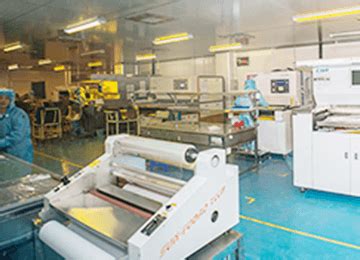
The manufacturing process of flex PCB cables is a sophisticated and intricate procedure that requires precision and expertise. Flex PCB cables, known for their flexibility and ability to fit into compact spaces, are essential components in modern electronic devices. Understanding the step-by-step process of their production provides insight into the complexity and innovation involved in creating these vital components.
The journey begins with the selection of materials.
The base material for flex PCBs is typically a flexible polymer, such as polyimide, which offers excellent thermal stability and flexibility. This material is chosen for its ability to withstand the mechanical stresses and environmental conditions that the final product will encounter. Once the base material is selected, a thin layer of copper foil is laminated onto it. This copper layer will form the conductive traces of the circuit.
Following the lamination, the next step is the application of a photoresist layer.
This light-sensitive material is applied to the copper surface to facilitate the patterning of the circuit. The photoresist is then exposed to ultraviolet light through a photomask, which contains the desired circuit pattern. The areas of the photoresist exposed to the light become hardened, while the unexposed areas remain soft and can be washed away. This process, known as photolithography, is crucial for defining the intricate circuit patterns on the flex PCB.
Once the photoresist has been developed, the exposed copper is etched away using a chemical solution, leaving behind the desired circuit pattern.
This etching process must be carefully controlled to ensure precision and accuracy, as any deviation can lead to defects in the final product. After etching, the remaining photoresist is removed, revealing the copper traces that form the circuit.
The next phase involves the application of a protective solder mask. This layer is applied over the copper traces to prevent oxidation and to protect against short circuits during soldering. The solder mask is typically a liquid polymer that is cured using ultraviolet light, providing a durable and protective coating.
Subsequently, the flex PCB undergoes a drilling process to create holes for component leads and vias, which are necessary for electrical connections between different layers of the circuit. These holes are drilled using precision machinery to ensure accuracy and alignment.
Following drilling, the flex PCB is plated with a thin layer of metal, usually nickel or gold, to enhance conductivity and provide a reliable surface for soldering components.
This plating process is essential for ensuring the longevity and performance of the flex PCB in its final application.
Finally, the flex PCB is subjected to a series of tests to verify its functionality and reliability.
These tests include electrical testing to ensure that the circuit is complete and free of defects, as well as mechanical testing to assess the flexibility and durability of the PCB. Once the flex PCB passes these rigorous tests, it is ready for integration into electronic devices.
In conclusion, the manufacturing process of flex PCB cables is a meticulous and highly technical procedure that involves multiple stages, each critical to the production of a reliable and high-quality product. From material selection to final testing, each step is carefully executed to ensure that the flex PCB meets the stringent requirements of modern electronic applications.
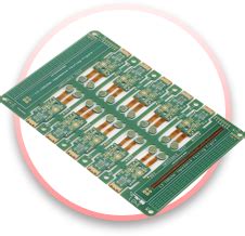
Common Challenges And Solutions In Flex PCB Cable Integration
Flex PCB cables, or flexible printed circuit board cables, have become increasingly integral in modern electronic devices due to their ability to bend and conform to various shapes, offering a versatile solution for compact and complex electronic assemblies. However, integrating these cables into electronic systems presents several challenges that require careful consideration and strategic solutions to ensure optimal performance and reliability.
One of the primary challenges in flex PCB cable integration is managing mechanical stress.
Due to their flexible nature, these cables are often subjected to bending, twisting, and other forms of mechanical manipulation. Over time, such stress can lead to material fatigue and eventual failure. To mitigate this issue, it is essential to design the flex PCB with appropriate bend radii and to use materials that can withstand repeated flexing. Additionally, incorporating strain relief features in the design can help distribute mechanical stress more evenly, thereby prolonging the lifespan of the cable.
Another significant challenge is ensuring signal integrity.
As electronic devices become more compact, the proximity of different signal paths within a flex PCB can lead to issues such as crosstalk and electromagnetic interference (EMI). To address these concerns, designers can employ techniques such as controlled impedance routing and the use of ground planes to minimize interference. Furthermore, selecting materials with suitable dielectric properties can enhance signal transmission and reduce the risk of signal degradation.
Thermal management is also a critical consideration in the integration of flex PCB cables.
The compact nature of these cables can lead to heat accumulation, which may affect the performance and reliability of the electronic system. Effective thermal management strategies, such as the use of thermal vias and heat spreaders, can help dissipate heat more efficiently. Additionally, choosing materials with high thermal conductivity can further aid in managing heat within the system.
The manufacturing process of flex PCB cables presents its own set of challenges.
Ensuring precision and accuracy during fabrication is crucial, as any defects can compromise the functionality of the cable. Advanced manufacturing techniques, such as laser cutting and automated optical inspection, can enhance the precision of the production process. Moreover, collaborating closely with experienced manufacturers can help identify potential issues early in the design phase, allowing for timely adjustments and improvements.
Cost considerations also play a significant role in the integration of flex PCB cables.
While these cables offer numerous advantages, their production can be more expensive than traditional rigid PCBs due to the complexity of their design and manufacturing processes. To address this, designers can optimize the layout to minimize material usage and reduce waste. Additionally, leveraging economies of scale by ordering larger quantities can help lower the overall cost per unit.
In conclusion, while the integration of flex PCB cables into electronic systems presents several challenges, these can be effectively managed through careful design, material selection, and collaboration with experienced manufacturers. By addressing mechanical stress, signal integrity, thermal management, manufacturing precision, and cost considerations, designers can harness the full potential of flex PCB cables, ensuring that they meet the demands of modern electronic applications. As technology continues to evolve, ongoing research and development in this field will likely yield new solutions and innovations, further enhancing the capabilities and applications of flex PCB cables in the future.

