Flex pcb gerber files
Understanding The Basics Of Flex PCB Gerber Files
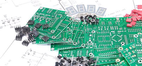
Flex PCB Gerber files are an essential component in the design and manufacturing process of flexible printed circuit boards (PCBs). These files serve as the blueprint for the production of PCBs, providing detailed instructions on how the board should be constructed. Understanding the basics of Flex PCB Gerber files is crucial for engineers and designers who work with flexible circuits, as these files ensure precision and accuracy in the manufacturing process.
To begin with, it is important to recognize that Gerber files are a standard format used in the PCB industry to convey information about the layout of a circuit board.
They are named after the Gerber Scientific Instrument Company, which developed the format. These files contain data about various layers of the PCB, including the copper layers, solder mask, silkscreen, and drill data. In the context of flex PCBs, Gerber files are particularly significant because they accommodate the unique properties and requirements of flexible circuits, which differ from those of rigid PCBs.
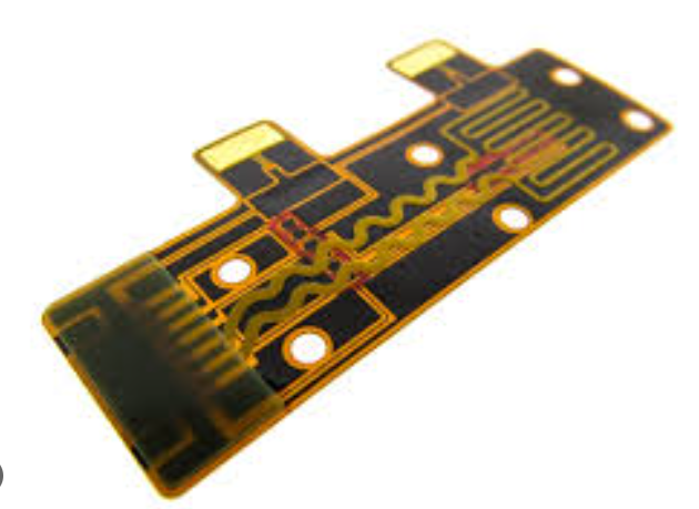
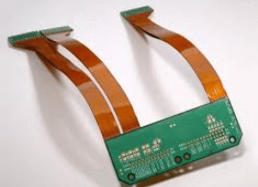
Flex PCBs are designed to be bent, twisted, and folded, allowing them to fit into compact spaces and conform to the shape of the device they are integrated into.
This flexibility necessitates a different approach to design and manufacturing, which is where Gerber files come into play. The files must accurately represent the flexible nature of the circuit, ensuring that the final product can withstand the mechanical stresses it will encounter in its application. Therefore, the creation of Flex PCB Gerber files requires careful consideration of factors such as bend radius, material properties, and the intended use of the circuit.
Moreover, the process of generating Gerber files for flex PCBs involves several steps.
Initially, designers use specialized software to create a digital representation of the circuit board. This design includes all the necessary components, traces, and connections. Once the design is complete, the software converts it into a series of Gerber files, each corresponding to a specific layer of the PCB. These files are then sent to the manufacturer, who uses them to produce the physical circuit board.
In addition to the standard layers found in rigid PCBs, flex PCBs may include additional layers or features to enhance their performance.
For instance, they might incorporate stiffeners to provide support in certain areas or use different materials to improve flexibility. These elements must be accurately represented in the Gerber files to ensure that the final product meets the desired specifications.
Furthermore, it is essential to verify the accuracy of Gerber files before they are sent to production.
This verification process, often referred to as a design rule check (DRC), involves reviewing the files to ensure that they comply with industry standards and the specific requirements of the project. Any errors or discrepancies identified during this process can be corrected before manufacturing begins, reducing the risk of costly mistakes and delays.
In conclusion, Flex PCB Gerber files play a vital role in the design and production of flexible printed circuit boards. They provide a detailed and precise representation of the circuit, ensuring that the final product meets the necessary specifications and can perform reliably in its intended application. By understanding the basics of these files, engineers and designers can create more effective and efficient flex PCBs, ultimately contributing to the advancement of technology in various industries.
Key Considerations When Designing Flex PCB Gerber Files
When designing flex PCB Gerber files, several key considerations must be taken into account to ensure the successful fabrication and functionality of the final product. Flex PCBs, or flexible printed circuit boards, offer unique advantages over traditional rigid PCBs, such as the ability to bend and conform to various shapes, making them ideal for compact and dynamic applications. However, the design process for flex PCBs requires careful attention to detail to address the specific challenges associated with their flexibility and material properties.
To begin with, understanding the material properties of flex PCBs is crucial.
Unlike rigid PCBs, flex PCBs are made from flexible substrates such as polyimide, which allows them to bend and twist. This flexibility, while advantageous, also introduces potential issues such as stress concentration and mechanical fatigue. Therefore, it is essential to consider the bending radius and the number of flex cycles the PCB will undergo during its lifetime. Designing with an appropriate bending radius can prevent cracking and ensure the longevity of the circuit.
Moreover, trace routing is another critical aspect of designing flex PCB Gerber files.
The traces on a flex PCB must be carefully routed to minimize stress and avoid potential failure points. It is advisable to use curved traces instead of sharp angles, as sharp angles can become stress concentrators and lead to trace cracking. Additionally, maintaining uniform trace widths and spacing can help distribute mechanical stress more evenly across the board. This consideration is particularly important in dynamic applications where the PCB will be subjected to repeated bending.
Transitioning to the topic of stack-up design, it is important to note that flex PCBs often consist of multiple layers.
The stack-up design should be optimized to balance flexibility with electrical performance. For instance, placing ground and power planes on separate layers can help reduce electromagnetic interference while maintaining the board’s flexibility. Furthermore, the use of adhesive layers should be minimized, as they can add stiffness to the board. Instead, relying on the inherent adhesive properties of the polyimide substrate can help maintain flexibility.
In addition to these considerations, the choice of coverlay material is also significant. Coverlays protect the copper traces on a flex PCB and provide insulation.
Selecting a coverlay material that matches the flexibility and thermal properties of the substrate is essential to prevent delamination and ensure reliable performance. Furthermore, the coverlay should be designed with appropriate openings to expose pads for soldering components, while also providing adequate protection to the traces.
Another important aspect to consider is the design of the Gerber files themselves.
Gerber files are the standard format for PCB design data and are used by manufacturers to fabricate the boards. Ensuring that the Gerber files are accurate and complete is vital for successful production. This includes verifying that all layers are correctly defined, including copper layers, solder mask, and silkscreen. Additionally, it is important to include detailed fabrication notes and specifications to guide the manufacturer in producing the flex PCB according to the design intent.
In conclusion, designing flex PCB Gerber files requires a comprehensive understanding of the unique challenges and considerations associated with flexible circuits. By carefully addressing material properties, trace routing, stack-up design, coverlay selection, and Gerber file accuracy, designers can create flex PCBs that meet the demands of modern electronic applications. Through meticulous planning and attention to detail, the potential of flex PCBs can be fully realized, offering innovative solutions for a wide range of industries.
Common Mistakes To Avoid In Flex PCB Gerber File Creation
Creating Gerber files for flex PCBs is a critical step in the design and manufacturing process, as these files serve as the blueprint for the production of printed circuit boards. However, several common mistakes can occur during this phase, potentially leading to costly errors and delays. Understanding these pitfalls and how to avoid them is essential for ensuring a smooth transition from design to production.
One frequent mistake in flex PCB Gerber file creation is the incorrect layer stack-up.
Flex PCBs often require a more complex layer configuration compared to rigid PCBs due to their flexible nature and specific application requirements. Designers must ensure that the layer stack-up in the Gerber files accurately reflects the intended design. This includes correctly defining the order and material of each layer, as well as any necessary adhesive or coverlay layers. Failing to do so can result in manufacturing issues, such as improper layer alignment or insufficient flexibility.
Another common error involves the misalignment of drill files with the corresponding Gerber files.
Drill files, which specify the locations and sizes of holes in the PCB, must be precisely aligned with the Gerber files to ensure accurate hole placement. Misalignment can lead to issues such as vias or mounting holes being drilled in the wrong locations, which can compromise the functionality of the PCB. To avoid this, designers should double-check the alignment of drill files with the Gerber files before submission.
Additionally, inadequate attention to design rules and constraints can lead to problems in flex PCB Gerber file creation.
Flex PCBs often have unique design requirements due to their ability to bend and flex. For instance, trace widths and spacing may need to be adjusted to accommodate the mechanical stresses that occur during flexing. Ignoring these constraints can result in broken traces or other mechanical failures. Therefore, it is crucial for designers to adhere to the specific design rules for flex PCBs and verify that these rules are reflected in the Gerber files.
Moreover, insufficient documentation and labeling within the Gerber files can cause confusion during the manufacturing process.
Each layer in the Gerber files should be clearly labeled, and any special instructions or notes should be included to guide the manufacturer. This is particularly important for flex PCBs, which may have unique requirements or features that need to be communicated clearly. Providing comprehensive documentation helps ensure that the manufacturer understands the design intent and can produce the PCB accurately.
Furthermore, neglecting to perform a thorough design review and simulation can lead to errors in the final product.
Before generating the Gerber files, designers should conduct a detailed review of the PCB design to identify any potential issues. This includes running simulations to test the electrical and mechanical performance of the design under various conditions. By identifying and addressing potential problems early in the design process, designers can reduce the risk of errors in the Gerber files.
In conclusion, while creating Gerber files for flex PCBs can be a complex task, being aware of common mistakes and taking steps to avoid them can significantly improve the chances of success. By ensuring accurate layer stack-up, aligning drill files correctly, adhering to design rules, providing clear documentation, and conducting thorough design reviews, designers can create Gerber files that accurately represent their flex PCB designs and facilitate a smooth manufacturing process.
Advanced Techniques For Optimizing Flex PCB Gerber Files
In the realm of modern electronics, the demand for compact, lightweight, and flexible devices has led to the increased utilization of flexible printed circuit boards (PCBs). These innovative circuits offer a myriad of advantages over their rigid counterparts, including enhanced flexibility, reduced weight, and the ability to conform to complex shapes. However, designing and optimizing flex PCB Gerber files, which are the standard format for PCB design data, requires a nuanced understanding of advanced techniques to ensure optimal performance and manufacturability.
To begin with, one of the primary considerations in optimizing flex PCB Gerber files is the careful management of trace routing.
Unlike rigid PCBs, flex circuits are subject to mechanical stress and bending, which can lead to trace cracking or delamination if not properly addressed. Therefore, it is crucial to employ curved trace routing instead of sharp angles, as this reduces stress concentration points. Additionally, maintaining consistent trace widths and spacing can help distribute mechanical loads more evenly across the circuit, thereby enhancing its durability.
Moreover, the choice of materials plays a pivotal role in the optimization process.
Flex PCBs typically utilize polyimide substrates due to their excellent thermal stability and flexibility. However, selecting the appropriate copper thickness is equally important. Thinner copper layers can improve flexibility but may compromise current-carrying capacity. Conversely, thicker copper can handle higher currents but may reduce the board’s flexibility. Striking a balance between these factors is essential for achieving a design that meets both electrical and mechanical requirements.
Another advanced technique involves the strategic placement of stiffeners.
Stiffeners are used to reinforce specific areas of a flex PCB, providing additional support where components are mounted or where connectors are attached. By incorporating stiffeners in the Gerber files, designers can ensure that these critical areas maintain their structural integrity during bending and flexing. This not only enhances the reliability of the circuit but also facilitates easier assembly and handling.
Furthermore, the implementation of controlled impedance is a critical aspect of optimizing flex PCB Gerber files, particularly for high-frequency applications.
Controlled impedance ensures that signal integrity is maintained across the circuit, minimizing issues such as signal reflection and crosstalk. To achieve this, designers must carefully calculate the trace width, spacing, and dielectric thickness, taking into account the specific material properties of the flex substrate. By incorporating these parameters into the Gerber files, designers can create circuits that perform reliably in demanding environments.
In addition to these technical considerations, collaboration with manufacturers during the design phase can significantly enhance the optimization of flex PCB Gerber files.
Manufacturers possess valuable insights into the capabilities and limitations of their fabrication processes, which can inform design decisions and prevent potential issues. By engaging in open communication with manufacturers, designers can ensure that their Gerber files are tailored to the specific requirements of the production process, ultimately leading to higher yields and reduced costs.
In conclusion, optimizing flex PCB Gerber files requires a comprehensive approach that encompasses trace routing, material selection, stiffener placement, controlled impedance, and collaboration with manufacturers. By employing these advanced techniques, designers can create flexible circuits that not only meet the stringent demands of modern electronic devices but also deliver exceptional performance and reliability. As the electronics industry continues to evolve, the ability to effectively optimize flex PCB designs will remain a critical skill for engineers and designers alike.