Flex pcb in kicad
Designing Flex PCBs in KiCad: A Step-by-Step Guide
Designing flexible printed circuit boards (PCBs) in KiCad requires a nuanced understanding of both the software and the unique characteristics of flex PCBs. As electronic devices become more compact and versatile, the demand for flexible PCBs has increased, necessitating a comprehensive approach to their design.KiCad, an open-source PCB design tool, offers a robust platform for creating these intricate circuits.
To begin with, it is essential to understand the fundamental differences between rigid and flexible PCBs.
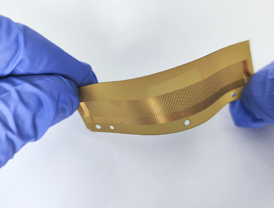
Flex PCBs are designed to bend and conform to specific shapes, which allows for more dynamic applications. This flexibility is achieved through the use of flexible substrates, such as polyimide, which can withstand bending and twisting without compromising the integrity of the circuit.
When embarking on the design process in KiCad, the first step is to set up the project environment.
This involves creating a new project and defining the board outline to match the desired shape of the flex PCB. KiCad’s board editor allows for precise control over the board’s dimensions and shape, which is crucial for ensuring that the final product fits within the intended application. Once the board outline is established, the next step is to import or create the schematic. The schematic serves as the blueprint for the circuit, detailing the connections between various components. In KiCad, this process is facilitated by the schematic editor, which provides a comprehensive library of components and symbols.
After the schematic is complete, the next phase involves laying out the components on the board.
This step is particularly critical for flex PCBs, as the placement of components can significantly impact the board’s flexibility and performance. KiCad’s layout editor offers tools for precise component placement and routing, allowing designers to optimize the board’s layout for both functionality and flexibility. It is important to consider the bending areas of the flex PCB during this stage, ensuring that components are not placed in regions that will experience significant stress.
Transitioning from layout to routing, designers must pay careful attention to the trace routing on a flex PCB.
The routing process in KiCad involves defining the paths for electrical connections between components. For flex PCBs, it is advisable to use curved traces instead of sharp angles, as this reduces stress concentrations and enhances the board’s durability. Additionally, maintaining consistent trace widths and spacing is crucial to prevent electrical interference and ensure reliable performance.
Once the routing is complete, the design must be thoroughly reviewed and verified.
KiCad provides tools for design rule checks (DRC) and electrical rule checks (ERC), which help identify potential issues before the board is manufactured. These checks are vital for ensuring that the design adheres to industry standards and will function as intended. After addressing any errors or warnings, the final step is to generate the necessary files for manufacturing. KiCad allows designers to export Gerber files, which are used by manufacturers to produce the physical PCB.
In conclusion, designing flex PCBs in KiCad involves a series of methodical steps, each requiring careful consideration and attention to detail. By understanding the unique requirements of flex PCBs and leveraging KiCad’s powerful tools, designers can create innovative and reliable circuits that meet the demands of modern electronic applications. Through meticulous planning and execution, the potential of flexible PCBs can be fully realized, paving the way for advancements in technology and design.

Best Practices for Flex PCB Layout in KiCad
Designing flexible printed circuit boards (PCBs) in KiCad requires a meticulous approach to ensure both functionality and reliability. As flexible PCBs are increasingly used in applications where space constraints and mechanical flexibility are paramount, understanding the best practices for their layout is essential. KiCad, an open-source PCB design tool, offers a robust platform for creating these intricate designs. However, to fully leverage its capabilities, designers must adhere to certain guidelines that optimize the performance and durability of flex PCBs.
To begin with, it is crucial to understand the unique characteristics of flex PCBs.
Unlike rigid PCBs, flex circuits are designed to bend and twist, which necessitates careful consideration of material properties and mechanical stresses. In KiCad, this begins with the selection of appropriate materials and stack-up configurations. Designers should choose materials that offer the necessary flexibility and thermal stability, such as polyimide substrates, which are commonly used in flex PCB applications.
Once the material selection is complete, the next step is to focus on the layout design.
In KiCad, it is advisable to use curved traces instead of sharp angles. This is because sharp angles can create stress points that may lead to cracking or delamination over time. By using smooth, curved traces, designers can distribute mechanical stress more evenly across the board. Additionally, maintaining consistent trace widths and spacing is vital to ensure signal integrity and prevent potential electrical issues.
Another important consideration is the placement of components. In flex PCB design, components should be strategically placed to minimize stress during bending.
It is recommended to place components in areas that experience minimal flexing, such as near the rigid sections of the board. KiCad allows designers to simulate mechanical stresses, which can be invaluable in identifying potential problem areas before the board is manufactured.
Furthermore, the use of teardrops at trace-to-pad junctions is a best practice that can enhance the durability of flex PCBs.
Teardrops provide additional support at these junctions, reducing the risk of trace lifting or cracking. KiCad’s design tools facilitate the easy implementation of teardrops, ensuring that these critical areas are reinforced.
In addition to these layout considerations, it is essential to incorporate appropriate design rules and constraints within KiCad.
Setting up these rules helps prevent common design errors and ensures that the final product meets the necessary specifications. For instance, specifying minimum bend radius constraints can prevent excessive bending that might damage the board.
Moreover, testing and validation are integral parts of the design process.
KiCad offers simulation tools that allow designers to test their layouts under various conditions, ensuring that the flex PCB will perform as expected in real-world applications. By thoroughly testing the design, potential issues can be identified and addressed early in the development process.
In conclusion, designing flex PCBs in KiCad requires a comprehensive understanding of both the software’s capabilities and the unique demands of flexible circuits. By adhering to best practices such as using curved traces, strategic component placement, and incorporating teardrops, designers can create reliable and efficient flex PCBs. Additionally, leveraging KiCad’s simulation and validation tools ensures that the final product will meet the necessary performance standards. Through careful planning and execution, designers can successfully navigate the complexities of flex PCB design in KiCad, resulting in innovative solutions for modern electronic applications.

Material Selection for Flex PCBs Using KiCad
When designing flexible printed circuit boards (PCBs) using KiCad, a comprehensive understanding of material selection is crucial to ensure optimal performance and reliability. Flex PCBs, known for their ability to bend and conform to various shapes, are increasingly used in applications where space constraints and mechanical flexibility are paramount. Therefore, selecting the appropriate materials is a critical step in the design process, as it directly impacts the board’s functionality and durability.
To begin with, the substrate material is a fundamental consideration in flex PCB design.
Polyimide is the most commonly used substrate due to its excellent thermal stability, mechanical strength, and flexibility. Its ability to withstand high temperatures makes it suitable for applications that require soldering processes. Additionally, polyimide’s low dielectric constant and loss tangent contribute to superior electrical performance, which is essential for high-frequency applications. In KiCad, designers can specify the substrate material properties to simulate and analyze the board’s behavior under various conditions, ensuring that the chosen material meets the design requirements.
Moreover, the choice of adhesive is another critical factor in flex PCB material selection.
Adhesives are used to bond the layers of the flex circuit, and their properties significantly affect the board’s flexibility and thermal performance. Acrylic and epoxy adhesives are commonly used, each offering distinct advantages. Acrylic adhesives provide excellent flexibility and are suitable for dynamic applications where the board will undergo repeated bending. On the other hand, epoxy adhesives offer superior thermal resistance, making them ideal for high-temperature environments. KiCad allows designers to incorporate these material properties into their simulations, enabling them to predict how different adhesives will perform in their specific applications.
In addition to substrate and adhesive materials, the selection of conductive materials is vital for ensuring reliable electrical performance.
Copper is the standard choice for conductive traces due to its excellent electrical conductivity and ductility. However, the thickness of the copper layer must be carefully considered, as it affects both the board’s flexibility and current-carrying capacity. Thinner copper layers enhance flexibility but may limit the amount of current the board can handle. KiCad’s design tools facilitate the optimization of trace thickness by allowing designers to simulate current flow and thermal effects, ensuring that the chosen copper thickness aligns with the application’s electrical requirements.
Furthermore, protective coatings play a significant role in safeguarding flex PCBs from environmental factors such as moisture, dust, and chemicals.
Polyimide coverlays and solder masks are commonly used to protect the circuit while maintaining flexibility. The choice between these coatings depends on the specific environmental conditions the PCB will encounter. KiCad’s design environment supports the integration of these protective layers, enabling designers to visualize and assess their impact on the overall board design.
In conclusion, material selection is a pivotal aspect of flex PCB design in KiCad, influencing the board’s mechanical, thermal, and electrical properties. By carefully choosing the substrate, adhesive, conductive materials, and protective coatings, designers can optimize their flex PCBs for a wide range of applications. KiCad’s robust simulation and design tools provide invaluable support in this process, allowing for precise material specification and performance analysis. As the demand for flexible electronics continues to grow, mastering material selection in KiCad will be essential for engineers seeking to create innovative and reliable flex PCB solutions.
Troubleshooting Common Issues in Flex PCB Design with KiCad
Designing flexible printed circuit boards (PCBs) using KiCad can be a rewarding endeavor, offering the potential for innovative and compact electronic solutions. However, like any design process, it is not without its challenges. Understanding and troubleshooting common issues that arise during the design of flex PCBs in KiCad is crucial for ensuring a successful outcome. By addressing these challenges systematically, designers can enhance the reliability and functionality of their projects.
One of the primary issues encountered in flex PCB design is the management of mechanical stress.
Flexible circuits are often subjected to bending and twisting, which can lead to mechanical failure if not properly accounted for. In KiCad, it is essential to accurately define the board outline and layer stack-up to reflect the intended flexing areas. This involves using the appropriate layer types and ensuring that the copper traces are routed in a manner that minimizes stress concentration. For instance, traces should be routed perpendicular to the bend lines and should avoid sharp angles, which can act as stress risers.
Another common challenge is ensuring signal integrity, particularly in high-speed applications.
Flex PCBs can introduce unique impedance characteristics due to their varying thickness and dielectric properties. In KiCad, designers should utilize the built-in tools to perform impedance calculations and adjust trace widths and spacing accordingly. Additionally, it is advisable to use ground planes and shielding techniques to mitigate electromagnetic interference (EMI), which can be more pronounced in flexible circuits due to their often compact and irregular shapes.
Thermal management is also a critical consideration in flex PCB design.
The flexible materials used in these circuits typically have lower thermal conductivity compared to rigid boards, which can lead to overheating issues. In KiCad, designers should carefully plan the placement of heat-generating components and consider the use of thermal vias and heat sinks to dissipate excess heat. Moreover, simulating thermal performance using KiCad’s integration with external simulation tools can provide valuable insights into potential hotspots and allow for preemptive design adjustments.
Component placement and routing present additional challenges in flex PCB design.
The limited space and unique form factors of flexible circuits require meticulous planning to ensure that all components fit within the designated areas without compromising functionality. KiCad offers a range of features to assist with this, including interactive routing and design rule checks that help maintain clearances and prevent short circuits. It is also beneficial to use 3D visualization tools within KiCad to verify component placement and ensure that the design will fit within the intended enclosure or application.
Finally, manufacturability is a crucial aspect that must be considered throughout the design process.
Flex PCBs often require specialized manufacturing processes, and it is important to communicate with fabricators early in the design phase to understand their capabilities and limitations. KiCad’s ability to generate detailed fabrication outputs, such as Gerber files and assembly drawings, facilitates this communication and helps ensure that the design can be manufactured as intended.
In conclusion, while designing flex PCBs in KiCad presents unique challenges, a methodical approach to troubleshooting common issues can lead to successful and innovative designs. By focusing on mechanical stress management, signal integrity, thermal performance, component placement, and manufacturability, designers can leverage KiCad’s powerful tools to create reliable and efficient flexible circuits.