Flexible pcb assembly process
Understanding The Basics Of Flexible PCB Assembly
Flexible PCB assembly is a critical process in the manufacturing of modern electronic devices, offering numerous advantages over traditional rigid PCBs. Understanding the basics of this process is essential for those involved in electronics design and production. Flexible PCBs, or flex circuits, are designed to bend and conform to specific shapes, making them ideal for applications where space is limited or where the circuit needs to fit into a non-linear configuration. This adaptability is achieved through the use of flexible substrates, such as polyimide, which provide the necessary durability and flexibility.
The assembly process of flexible PCBs begins with the design phase, where engineers create a layout that maximizes the benefits of the flexible material.
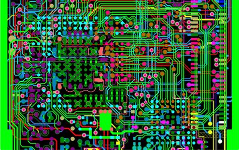
This involves careful consideration of the circuit’s routing, component placement, and the mechanical stresses the board will endure. Once the design is finalized, the manufacturing process can commence. The first step in manufacturing is the fabrication of the flexible substrate, which involves layering the polyimide material with copper to form the conductive traces. This is typically done using a process called photolithography, where a photoresist is applied to the substrate, exposed to light through a mask, and then developed to reveal the desired circuit pattern.
Following the fabrication of the substrate, the next step is the application of surface finishes to protect the copper traces and ensure reliable soldering.
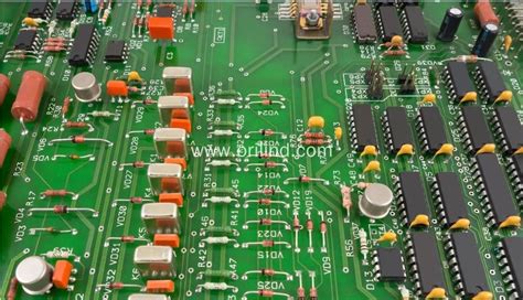
Common finishes include immersion gold, immersion silver, and organic solderability preservatives (OSP). These finishes help prevent oxidation and improve the solderability of the board. Once the surface finish is applied, the board is ready for component placement. This step is similar to that of rigid PCB assembly, where components are placed onto the board using automated pick-and-place machines. However, the flexible nature of the substrate requires special handling to prevent damage during this process.
Soldering is the next critical step in the assembly process.
Flexible PCBs often use surface mount technology (SMT) for component attachment, which involves applying solder paste to the board, placing components, and then passing the assembly through a reflow oven. The heat from the oven melts the solder paste, creating a strong bond between the components and the board. Due to the heat-sensitive nature of flexible substrates, precise temperature control is essential to prevent warping or damage.
After soldering, the assembled flexible PCB undergoes inspection and testing to ensure functionality and reliability.
Automated optical inspection (AOI) systems are commonly used to check for defects such as misaligned components or solder bridges. Electrical testing is also performed to verify that the circuit functions as intended. Any defects identified during these inspections must be addressed before the board can proceed to the final stages of production.
Finally, the completed flexible PCB is subjected to additional processes such as encapsulation or conformal coating, which provide additional protection against environmental factors like moisture and dust. These coatings are particularly important for applications where the board will be exposed to harsh conditions. In conclusion, the flexible PCB assembly process is a complex and precise operation that requires careful planning and execution. By understanding the intricacies of this process, manufacturers can produce high-quality flexible circuits that meet the demanding requirements of modern electronic devices.
Key Advantages Of Using Flexible PCBs In Modern Electronics
Flexible printed circuit boards (PCBs) have become an integral component in the design and manufacturing of modern electronic devices, offering a multitude of advantages that cater to the evolving demands of technology. As electronic devices continue to shrink in size while expanding in functionality, the need for components that can accommodate these changes has become increasingly critical. Flexible PCBs, with their unique properties, provide a solution that addresses these challenges effectively.
One of the primary advantages of flexible PCBs is their ability to conform to complex shapes and fit into compact spaces.
Unlike traditional rigid PCBs, flexible circuits can be bent, folded, and twisted without compromising their functionality. This adaptability allows designers to create more innovative and compact electronic devices, such as wearable technology, medical implants, and advanced communication devices. The ability to fit into unconventional spaces not only enhances the aesthetic appeal of the devices but also contributes to their overall performance by reducing the need for additional connectors and interconnects.
In addition to their physical flexibility, flexible PCBs offer significant weight and space savings.
By eliminating the need for bulky connectors and reducing the number of components required, these circuits contribute to the miniaturization of electronic devices. This reduction in size and weight is particularly beneficial in applications where portability is crucial, such as in aerospace and automotive industries. Furthermore, the streamlined design of flexible PCBs can lead to improved signal integrity and reduced electromagnetic interference, enhancing the reliability and efficiency of the devices in which they are used.
Another notable advantage of flexible PCBs is their durability and resilience.
These circuits are designed to withstand harsh environmental conditions, including extreme temperatures, vibrations, and exposure to chemicals. This robustness makes them ideal for use in demanding applications, such as industrial machinery and military equipment, where reliability is paramount. The materials used in flexible PCBs, such as polyimide and polyester, provide excellent thermal stability and resistance to wear and tear, ensuring a longer lifespan for the electronic devices.
Moreover, the manufacturing process of flexible PCBs is highly efficient and cost-effective.
The ability to produce these circuits in large volumes with minimal material waste contributes to a reduction in production costs. Additionally, the simplified assembly process, which often involves fewer components and connections, further reduces labor costs and assembly time. This efficiency not only benefits manufacturers but also translates to cost savings for consumers, making advanced electronic devices more accessible to a broader audience.
Furthermore, flexible PCBs support the growing trend towards environmentally friendly electronics.
The reduction in material usage and waste during production aligns with sustainable manufacturing practices. Additionally, the longer lifespan and enhanced reliability of devices using flexible PCBs contribute to a decrease in electronic waste, supporting global efforts to minimize the environmental impact of technology.
In conclusion, the key advantages of using flexible PCBs in modern electronics are manifold. Their adaptability, space and weight efficiency, durability, cost-effectiveness, and environmental benefits make them an indispensable component in the development of cutting-edge electronic devices. As technology continues to advance, the role of flexible PCBs is likely to expand, driving innovation and enabling the creation of more sophisticated and sustainable electronic solutions.
Challenges And Solutions In Flexible PCB Manufacturing
The flexible PCB assembly process presents a unique set of challenges and solutions that are critical to the advancement of modern electronics. As technology continues to evolve, the demand for smaller, lighter, and more versatile electronic devices has led to the increased use of flexible printed circuit boards (PCBs). These boards offer significant advantages over their rigid counterparts, including the ability to bend and conform to various shapes, which is essential for applications in wearable technology, medical devices, and other compact electronic systems. However, the manufacturing of flexible PCBs is not without its difficulties.
One of the primary challenges in flexible PCB manufacturing is the material selection.
Unlike rigid PCBs, which are typically made from fiberglass-reinforced epoxy, flexible PCBs use materials such as polyimide or polyester films. These materials must possess excellent thermal stability, mechanical flexibility, and electrical insulation properties. Selecting the appropriate material is crucial, as it directly impacts the board’s performance and reliability. To address this challenge, manufacturers often conduct extensive testing and evaluation of different materials to ensure they meet the specific requirements of the intended application.
Another significant challenge is the handling and processing of flexible substrates.
Due to their thin and pliable nature, flexible PCBs are more susceptible to damage during the manufacturing process. This vulnerability necessitates the use of specialized equipment and techniques to prevent tearing, creasing, or other forms of mechanical stress. For instance, manufacturers may employ automated handling systems that minimize human contact with the boards, thereby reducing the risk of damage. Additionally, the use of precision alignment tools and fixtures can help maintain the integrity of the flexible substrates throughout the assembly process.
The soldering process also presents unique challenges in flexible PCB assembly.
The heat-sensitive nature of flexible materials requires careful control of temperature and soldering time to prevent damage. Traditional soldering techniques, such as wave soldering, may not be suitable for flexible PCBs due to the risk of thermal stress. Instead, manufacturers often use reflow soldering with controlled temperature profiles or employ alternative methods like conductive adhesives. These solutions help ensure reliable electrical connections without compromising the structural integrity of the flexible board.
Moreover, the inspection and testing of flexible PCBs pose additional challenges.
The flexibility of these boards can make it difficult to perform standard testing procedures, such as automated optical inspection (AOI) or in-circuit testing (ICT). To overcome this, manufacturers may develop custom fixtures and testing protocols tailored to the specific design and application of the flexible PCB. Advanced imaging techniques, such as X-ray inspection, can also be employed to detect defects that are not visible through traditional methods.
In conclusion, while the flexible PCB assembly process presents several challenges, innovative solutions and advancements in technology continue to drive progress in this field. By carefully selecting materials, employing specialized handling and soldering techniques, and developing customized testing protocols, manufacturers can overcome these obstacles and produce high-quality flexible PCBs. As the demand for flexible electronics continues to grow, ongoing research and development will undoubtedly lead to further improvements in the manufacturing process, enabling the creation of even more sophisticated and reliable electronic devices.
Innovations In Flexible PCB Assembly Techniques
The field of flexible printed circuit board (PCB) assembly has witnessed significant advancements in recent years, driven by the increasing demand for compact, lightweight, and versatile electronic devices. As technology continues to evolve, the need for innovative assembly techniques becomes paramount to accommodate the unique characteristics of flexible PCBs. These circuits, unlike their rigid counterparts, offer the advantage of bending and folding, which allows for more creative and space-efficient designs. Consequently, the assembly process must adapt to these features to ensure reliability and performance.
One of the primary innovations in flexible PCB assembly is the development of advanced surface mount technology (SMT) techniques.
SMT has long been a staple in PCB assembly due to its efficiency and ability to accommodate miniaturized components. However, when applied to flexible substrates, traditional SMT processes require modifications to address the challenges posed by the material’s pliability. For instance, the use of low-temperature soldering techniques has become increasingly prevalent. These methods reduce the thermal stress on the flexible substrate, thereby minimizing the risk of warping or damage during assembly. Additionally, specialized adhesives and conductive pastes are employed to enhance the mechanical and electrical connections between components and the flexible board.
Moreover, the integration of automated optical inspection (AOI) systems has revolutionized quality control in flexible PCB assembly
. Given the delicate nature of flexible circuits, ensuring the accuracy and precision of component placement is crucial. AOI systems utilize high-resolution cameras and sophisticated algorithms to detect defects such as misalignments, soldering errors, and surface irregularities. This technology not only enhances the reliability of the final product but also reduces the time and cost associated with manual inspection processes. As a result, manufacturers can achieve higher yields and maintain stringent quality standards.
In addition to these advancements, the adoption of laser-based technologies has further refined the flexible PCB assembly process.
Laser direct structuring (LDS) is one such technique that has gained traction. LDS allows for the creation of intricate circuit patterns directly onto the flexible substrate without the need for traditional etching processes. This method not only streamlines production but also enables greater design flexibility, as it supports the integration of complex geometries and fine pitch components. Furthermore, laser soldering techniques have emerged as a viable alternative to conventional soldering methods. By providing precise heat application, laser soldering minimizes thermal impact on the flexible substrate, thereby preserving its integrity and enhancing the overall durability of the assembly.
As the demand for flexible electronics continues to grow, the importance of innovative assembly techniques cannot be overstated.
The advancements in SMT, AOI, and laser-based technologies represent just a few of the many strides being made in this dynamic field. These innovations not only address the unique challenges associated with flexible PCBs but also pave the way for new applications and possibilities in various industries, including consumer electronics, automotive, and healthcare. By embracing these cutting-edge techniques, manufacturers can ensure that flexible PCBs meet the ever-evolving requirements of modern electronic devices, ultimately contributing to the advancement of technology as a whole