Streamlining SMT Assembly with EasyEDA for Efficient PCB Design
Key Takeaways
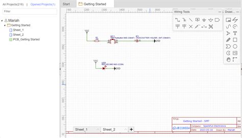
The success of PCB assembly processes heavily relies on efficient tools and methodologies. EasyEDA stands out as a pivotal platform that simplifies and enhances SMT assembly, making it easier for designers to transition from prototype to production seamlessly. One of the primary advantages of utilizing EasyEDA is its intuitive interface, which allows users to design, simulate, and prepare for PCBA in a cohesive environment.
Incorporating features such as real-time collaboration and integrated component libraries, EasyEDA facilitates more effective communication among team members—crucial when working on SMT assembly projects that require precision and speed. Moreover, its simulation tools help identify potential issues early in the design phase, which significantly reduces the time spent on revisions during the actual assembly process.
To summarize these benefits, consider the table below that outlines how EasyEDA enhances various aspects of PCBA:
| Feature | Benefit |
|---|---|
| Intuitive Design Interface | Eases the learning curve for new users |
| Integrated Component Library | Saves time sourcing components |
| Real-Time Collaboration | Increases team efficiency and reduces errors |
| Online Simulation Tools | Helps detect design flaws early |
By leveraging these capabilities of EasyEDA, teams can expect not only to speed up their PCB assembly efforts but also to improve the overall quality of their designs. This focus on efficiency ultimately leads to faster project completion while ensuring a high standard of output in SMT assembly.
Introduction to SMT Assembly and PCB Design
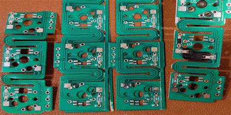
Surface Mount Technology (SMT) assembly has revolutionized the world of PCB design, making it possible to create smaller, more efficient circuit boards. As electronic devices continue to become more compact and powerful, the demand for efficient pcb assembly processes has never been greater. In this context, EasyEDA emerges as a valuable tool. It not only facilitates the design of printed circuit boards (PCBs) but also streamlines the assembly of components through its intuitive interfaces and integrated features. The combination of EasyEDA’s robust design capabilities with its support for efficient pcba processes ensures that engineers can execute their projects more swiftly and with heightened accuracy. By utilizing EasyEDA, designers can harness features like design simulation and a comprehensive part library, thereby significantly reducing errors and enhancing overall productivity in SMT assembly. Additionally, this platform supports collaboration, allowing teams to work closely together on designs before moving on to assembly, which in turn facilitates a smoother transition from concept to PCBA completion. Ultimately, understanding the importance of these modern tools in PCB design enables engineers to embrace efficiency and innovation in their work.
The Role of EasyEDA in Streamlining SMT Assembly
In today’s fast-paced electronics market, the integration of tools like EasyEDA has revolutionized the way designers approach SMT assembly and PCB design. The versatility and user-friendliness of EasyEDA provide a comprehensive solution that significantly enhances the pcb assembly process. One of the primary advantages of using EasyEDA lies in its ability to seamlessly blend design and manufacturing, which ensures that all elements of the pcba are accounted for from the start. By offering a vast library of components and an intuitive interface, users can quickly sketch out their ideas, allowing for rapid prototyping and iteration. This not only reduces time-to-market but also minimizes errors typically associated with manual designs. Furthermore, EasyEDA’s simulation tools enable designers to preemptively identify potential issues in their assembly plans before they reach physical production, streamlining workflows even further. Ultimately, leveraging these features allows teams to focus on innovation rather than getting bogged down in tedious logistics, leading to more efficient project completion and a stronger competitive edge in an ever-evolving landscape.
Key Features of EasyEDA for Efficient PCB Design
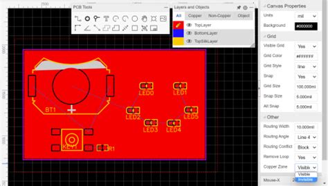
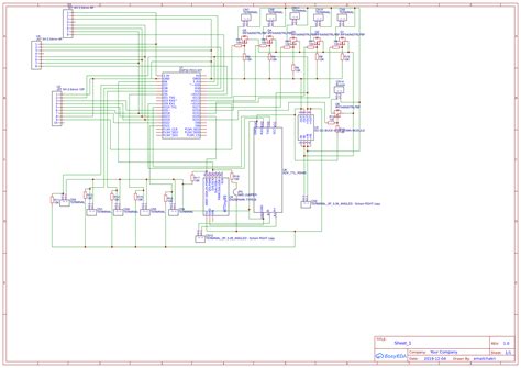
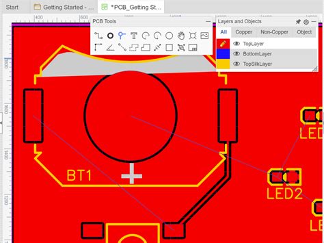
EasyEDA offers an array of powerful tools designed specifically to optimize the PCB assembly process, making it a standout choice for engineers and designers. One of the most notable features is its integrated design environment, which allows users to create schematics and PCB layouts within a single interface. This seamless interaction not only boosts productivity but also helps in reducing errors that may occur when switching between different software platforms. Furthermore, EasyEDA supports exporting designs for PCBA fabrication directly, streamlining the workflow from conceptualization to production.
Another significant advantage is its extensive library of components, which simplifies the selection process for parts necessary in a project. By having access to pre-defined libraries with various PCB assembly components, engineers can rapidly prototype and validate their designs without spending excessive time on part sourcing. Moreover, EasyEDA facilitates collaboration among team members through its cloud-based infrastructure, allowing multiple users to work on a design simultaneously. This feature enhances communication and ensures that everyone stays aligned during the development cycle. With tools tailored for simulation and analysis, EasyEDA empowers users to test different configurations virtually before finalizing designs for PCBA, minimizing the likelihood of costly mistakes in later stages of production.
In summary, the features offered by EasyEDA—ranging from its integrated design environment to collaborative capabilities—play a crucial role in making efficient PCB design accessible and manageable. By leveraging these tools effectively, users can significantly improve their workflow and achieve quicker turnaround times on their projects.
Practical Tips for Using EasyEDA in SMT Assembly
To maximize the potential of EasyEDA in your SMT assembly processes, there are several practical tips that can enhance your overall efficiency in PCB assembly. First and foremost, ensure that you are familiar with the user interface. A solid understanding of the available tools can dramatically reduce the time needed to design and prototype your PCBA. Utilize the component library extensively, as EasyEDA offers a vast selection of components that can save time during the design phase. This not only streamlines the process but also increases accuracy in component selection.
Furthermore, take advantage of EasyEDA’s simulation tools to pre-test and validate your designs before moving on to assembly. This reduces expensive errors that can occur later in production. It’s also advisable to optimize your layout for space efficiency, which is crucial for successful SMT assembly. Prioritize placing components that are likely to be soldered at similar times close together—this minimizes handling and can lead to a more efficient process.
“Always review your design rule checks (DRC) within EasyEDA before finalizing your project; it may save you from unexpected surprises down the line.”
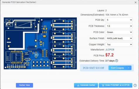
When you’re ready to move from design to actual PCBA, consider using EasyEDA’s export options carefully. Ensure that files are formatted correctly for your assembly service provider; this will help avoid delays that stem from incompatible file types.
In summary, by navigating the features of EasyEDA thoughtfully, applying design best practices, and utilizing available resources effectively, you can significantly improve not only your speed but also the quality of your final product during SMT assembly.
Enhancing Collaboration with EasyEDA Tools
Effective collaboration is pivotal in ensuring the success of pcb assembly projects. EasyEDA offers a range of tools that facilitate seamless teamwork, allowing multiple users to work on the same PCB design concurrently. This collaborative environment is strengthened by features such as real-time sharing, version control, and integrated communication channels that keep all team members informed and engaged throughout the design and assembly process. By leveraging these tools, teams can reduce the likelihood of errors and discrepancies that often arise in traditional pcb assembly methods. Furthermore, the intuitive interface of EasyEDA makes it easy for both experienced designers and newcomers to contribute to projects, fostering a spirit of cooperation and innovation. With features designed specifically for pcba processes, including automated design rule checks and instant feedback on layout modifications, teams can enhance both productivity and creativity while minimizing time-to-market. Consequently, integrating EasyEDA into your workflow not only streamlines project management but also elevates the overall quality of the final product.
Case Studies: Successful Projects Using EasyEDA
In exploring the transformational impact of EasyEDA on PCB assembly, numerous case studies demonstrate its practical applications and benefits. For instance, a small electronics startup utilized EasyEDA to transition from a traditional design approach to a more integrated PCBA method, significantly reducing their development time. By leveraging EasyEDA’s user-friendly interface, the team streamlined their workflow, allowing for easy creation and modification of designs while simultaneously managing component specifications. Another notable example is a medium-sized firm that faced challenges in scalability and production efficiency. With EasyEDA, they optimized their PCB assembly process by implementing its comprehensive simulation tools, which allowed them to identify potential design flaws before physical production. As a result, not only did they minimize errors during assembly, but they also achieved a remarkable reduction in material waste and production costs. These case studies highlight how EasyEDA’s robust features enable companies to enhance their PCB design efficiency while tackling the complexities associated with modern PCBA demands. By integrating technology into their workflow, these organizations have set benchmarks for achieving excellence in smt assembly, paving the way for others to follow suit in transforming their own practices through innovative tools like EasyEDA.
Future Trends in SMT Assembly and PCB Design
As technology continues to evolve, so do the methodologies associated with SMT assembly and PCB design. One prominent trend is the increasing integration of automation into the pcba process. Automation not only enhances the speed of assembly but also improves accuracy, allowing for more complex designs to be executed flawlessly. Furthermore, as manufacturing moves towards greater efficiency, the need for real-time data analysis grows. Tools like EasyEDA streamline this by providing immediate feedback and monitoring capabilities during the assembly process.
Another trend is the growing emphasis on sustainability within pcb assembly practices. Manufacturers are seeking eco-friendly materials and processes that minimize waste, which aligns well with consumer expectations for responsible production practices. EasyEDA provides resources that support these sustainable methods by allowing designers to simulate and optimize their layouts, reducing material usage without sacrificing quality.
Additionally, collaborative platforms are transforming how teams approach pcba projects. With EasyEDA’s shared workspace capabilities, teams can work together across geographical boundaries in real-time, promoting innovation through collective input and instant feedback. This shift towards collaboration is predicted to not only enhance project outcomes but also reduce time-to-market significantly.
In conclusion, staying informed about these emerging trends in SMT assembly and PCB design, along with utilizing intuitive tools like EasyEDA, will be crucial for engineers and designers looking to succeed in an increasingly competitive landscape. The future promises a more integrated, sustainable, and collaborative approach that can ultimately lead to enhanced productivity and innovation in electronic manufacturing.
Conclusion: Maximizing Efficiency with EasyEDA
In the realm of PCB assembly (pcba), the integration of modern tools has become crucial for achieving greater efficiency and effectiveness. EasyEDA has established itself as a vital resource in this transformation, allowing engineers and designers to streamline their workflows significantly. By utilizing EasyEDA’s features, users can see a reduction in assembly time while simultaneously elevating the quality of their designs. The tools within EasyEDA facilitate easier communication among team members, reduce the potential for errors, and enable faster iterations on designs, ultimately contributing to a more seamless SMT assembly process. The aforementioned advantages not only lead to enhanced productivity but also result in cost savings and timely project completions, making EasyEDA an indispensable player in the pcb assembly landscape. As industries continue to evolve, those who leverage such platforms will undoubtedly lead the way toward more innovative and efficient pcba solutions.
Conclusion: Maximizing Efficiency with EasyEDA
In summary, leveraging EasyEDA for SMT assembly presents a significant opportunity to enhance PCB design efficiency. By integrating its sophisticated tools and intuitive interface, users can simplify the pcb assembly process while improving accuracy and reducing lead times. The ability to efficiently manage designs not only streamlines workflows but also fosters collaboration among team members involved in the project. Emphasizing the use of proper techniques within EasyEDA can lead to faster iterations and refined results in PCBA projects. As the industry evolves, adopting platforms like EasyEDA will become increasingly essential for engineers looking to remain competitive and responsive to market demands. Embracing these practices ultimately results in better resource utilization and more successful project outcomes, showcasing how a focus on efficient design methods can yield substantial benefits for businesses engaged in electronics manufacturing.
FAQs
What is PCB assembly and why is it important?
PCB assembly, or PCBA, refers to the process of soldering electronic components onto a printed circuit board (PCB). This process is crucial as it directly impacts the functionality and reliability of electronic devices.
How can EasyEDA help in the PCB assembly process?
EasyEDA provides a range of tools designed to simplify the PCB assembly workflow. Features like schematic capture, simulation capabilities, and integrated manufacturing options help users streamline their design processes, making project completion quicker and more efficient.
What are some key features of EasyEDA that enhance PCB design efficiency?
Key features include real-time collaboration tools, extensive libraries of components, and automated error checking mechanisms. These functionalities collectively make it easier for teams to design effective PCBs with fewer errors during the SMT assembly stage.
Are there any specific techniques for optimizing SMT assembly with EasyEDA?
Yes, utilizing EasyEDA’s design rule checks (DRCs) ensures that your designs are manufacturable. Additionally, making use of their component placement features can significantly enhance alignment during SMT assembly, leading to better overall performance.
Can collaboration be improved using EasyEDA in the PCB design process?
Absolutely! EasyEDA’s cloud-based platform allows multiple users to work on a project simultaneously from different locations. This facilitates efficient teamwork and ensures everyone is on the same page during development and PCBA, increasing project speed and coherence.