Hdi flexible pcb
Advantages Of HDI Flexible PCBs In Modern Electronics
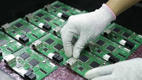
High-Density Interconnect (HDI) flexible printed circuit boards (PCBs) have emerged as a pivotal innovation in the realm of modern electronics, offering a multitude of advantages that cater to the ever-evolving demands of contemporary technology. As electronic devices continue to shrink in size while expanding in functionality, the need for compact, efficient, and reliable circuit solutions has become paramount. HDI flexible PCBs address these needs by providing a versatile platform that combines the benefits of high-density interconnectivity with the adaptability of flexible substrates.
One of the primary advantages of HDI flexible PCBs is their ability to support miniaturization.
As electronic devices become increasingly compact, the internal components must also be reduced in size without compromising performance. HDI technology allows for the integration of more components in a smaller area by utilizing finer lines and spaces, smaller vias, and higher connection pad density. This capability is particularly beneficial in applications such as smartphones, wearable devices, and medical implants, where space is at a premium and performance cannot be sacrificed.
In addition to facilitating miniaturization, HDI flexible PCBs offer enhanced electrical performance.
The reduced size of the interconnects and the shorter distances between components result in lower signal loss and improved signal integrity. This is crucial in high-speed applications where maintaining signal quality is essential for optimal device functionality. Furthermore, the use of microvias in HDI designs reduces parasitic inductance and capacitance, contributing to better overall electrical performance.
Another significant advantage of HDI flexible PCBs is their inherent flexibility, which allows for innovative design possibilities.
Unlike rigid PCBs, flexible circuits can be bent, folded, or twisted to fit into unconventional spaces, making them ideal for applications where traditional circuit boards would be impractical. This flexibility not only enables more creative product designs but also enhances the durability of the device by allowing it to withstand mechanical stress and vibration. Consequently, HDI flexible PCBs are increasingly utilized in automotive, aerospace, and industrial applications where reliability under dynamic conditions is critical.
Moreover, HDI flexible PCBs contribute to cost efficiency in the manufacturing process.
By reducing the number of layers required for complex circuits, they can lower material costs and simplify assembly processes. The ability to integrate multiple functions into a single flexible board also reduces the need for additional components and connectors, further decreasing production expenses. This cost-effectiveness, combined with the performance benefits, makes HDI flexible PCBs an attractive option for manufacturers seeking to optimize their products.
In conclusion, the advantages of HDI flexible PCBs in modern electronics are manifold, encompassing miniaturization, enhanced electrical performance, design flexibility, and cost efficiency. As technology continues to advance, the demand for compact, high-performance electronic solutions will only grow, solidifying the role of HDI flexible PCBs as a cornerstone of innovation. By enabling the development of smaller, more powerful, and more reliable devices, these advanced circuit boards are poised to play a crucial role in shaping the future of electronics. As such, their adoption across various industries is likely to accelerate, driven by the relentless pursuit of technological excellence and the ever-increasing expectations of consumers.
Design Considerations For HDI Flexible PCBs
When designing High-Density Interconnect (HDI) flexible printed circuit boards (PCBs), several critical considerations must be taken into account to ensure optimal performance and reliability. HDI flexible PCBs are increasingly favored in advanced electronic applications due to their ability to accommodate complex circuitry in compact spaces, offering both flexibility and high interconnect density. As such, understanding the nuances of their design is essential for engineers and designers aiming to leverage their full potential.
To begin with, material selection is a fundamental aspect of HDI flexible PCB design.
The choice of substrate material significantly influences the board’s flexibility, thermal performance, and overall durability. Polyimide is commonly used due to its excellent thermal stability and flexibility, which are crucial for applications that require bending and folding. However, the specific application requirements may necessitate alternative materials that offer different mechanical or thermal properties. Therefore, a thorough evaluation of the material’s characteristics in relation to the intended application is imperative.
Transitioning to the layout design, the miniaturization of components in HDI flexible PCBs demands meticulous attention to detail.
The use of microvias, which are smaller than traditional vias, is a hallmark of HDI technology. These microvias enable higher routing density by allowing more interconnections within a given area. However, their implementation requires precise drilling techniques and careful consideration of the aspect ratio to maintain structural integrity. Additionally, the placement of components must be strategically planned to minimize stress on the flexible areas, thereby preventing potential damage during bending or flexing.
Signal integrity is another critical consideration in the design of HDI flexible PCBs.
As the density of interconnections increases, so does the potential for signal interference and loss. To mitigate these issues, designers must employ advanced techniques such as controlled impedance routing and differential pair routing. These methods help maintain signal quality by reducing electromagnetic interference and ensuring consistent signal transmission. Furthermore, the use of ground planes and shielding can provide additional protection against external noise, thereby enhancing the overall performance of the circuit.
Thermal management is equally important in the design of HDI flexible PCBs.
The compact nature of these boards can lead to increased heat generation, which, if not properly managed, can adversely affect the performance and longevity of the components. Effective thermal management strategies include the use of thermal vias, heat sinks, and thermal interface materials to dissipate heat efficiently. Additionally, the layout should be optimized to facilitate natural airflow and heat distribution, thereby preventing hotspots and ensuring uniform temperature across the board.
Finally, manufacturability and cost considerations must not be overlooked.
The complexity of HDI flexible PCBs can lead to increased manufacturing challenges and costs. Therefore, collaboration with experienced manufacturers during the design phase is crucial to identify potential issues and optimize the design for cost-effective production. This includes selecting appropriate manufacturing processes, such as laser drilling for microvias and precision etching for fine lines, to ensure high-quality output.
In conclusion, the design of HDI flexible PCBs requires a comprehensive approach that addresses material selection, layout design, signal integrity, thermal management, and manufacturability. By carefully considering these factors, designers can create robust and efficient HDI flexible PCBs that meet the demands of modern electronic applications.
Manufacturing Process Of HDI Flexible PCBs
The manufacturing process of High-Density Interconnect (HDI) flexible printed circuit boards (PCBs) is a sophisticated and intricate procedure that requires precision and advanced technology. HDI flexible PCBs are renowned for their ability to accommodate complex circuitry in compact spaces, making them indispensable in modern electronic devices. To understand the manufacturing process, it is essential to explore the various stages involved, each contributing to the overall functionality and reliability of the final product.
Initially, the process begins with the selection of appropriate materials.
The base material for HDI flexible PCBs typically consists of a flexible substrate, such as polyimide, which offers excellent thermal stability and flexibility. This substrate is crucial as it allows the PCB to bend and conform to different shapes, a characteristic that is highly valued in applications where space is limited. Once the substrate is chosen, a thin layer of copper is laminated onto it, serving as the conductive layer for the circuit.
Following the material selection, the next step involves the design and layout of the circuit.
Advanced computer-aided design (CAD) software is employed to create intricate circuit patterns that meet the specific requirements of the application. This design phase is critical, as it determines the efficiency and performance of the PCB. Once the design is finalized, it is transferred onto the copper layer using a photolithographic process. This involves coating the copper with a photosensitive material, exposing it to ultraviolet light through a mask of the circuit pattern, and then developing it to reveal the desired circuit paths.
Subsequently, the exposed copper is etched away, leaving behind the precise circuit pattern on the flexible substrate.
This etching process is meticulously controlled to ensure that the circuit paths are accurate and free from defects. After etching, the PCB undergoes a series of cleaning processes to remove any residual chemicals and debris, ensuring a pristine surface for further processing.
The next phase involves the creation of vias, which are small holes that allow electrical connections between different layers of the PCB.
In HDI flexible PCBs, microvias are commonly used due to their ability to provide high-density interconnections. These microvias are typically formed using laser drilling, a technique that offers precision and control over the size and placement of the vias. Once the vias are drilled, they are plated with copper to establish electrical connectivity between the layers.
Following the via formation, additional layers of circuitry may be added, depending on the complexity of the design.
This is achieved through a process known as sequential lamination, where additional layers of copper and dielectric material are laminated onto the existing structure. Each new layer undergoes the same patterning, etching, and via formation processes, gradually building up the multi-layered structure of the HDI flexible PCB.
Finally, the PCB is subjected to a series of tests to verify its functionality and reliability.
These tests include electrical testing to ensure proper connectivity and performance, as well as mechanical testing to assess the flexibility and durability of the board. Once the PCB passes these rigorous tests, it is ready for integration into electronic devices.
In conclusion, the manufacturing process of HDI flexible PCBs is a complex and precise operation that involves multiple stages, each contributing to the creation of a high-performance and reliable product. From material selection to final testing, every step is carefully executed to meet the demanding requirements of modern electronic applications.
Applications Of HDI Flexible PCBs In Various Industries
High-Density Interconnect (HDI) flexible printed circuit boards (PCBs) have emerged as a pivotal technology in the electronics industry, offering a multitude of applications across various sectors. These advanced PCBs are characterized by their ability to accommodate a higher density of components on a smaller board, thanks to their fine lines and spaces, microvias, and high-performance materials. As industries continue to demand more compact, efficient, and reliable electronic solutions, HDI flexible PCBs have become indispensable.
In the consumer electronics industry, HDI flexible PCBs are widely used due to their ability to support the miniaturization of devices.
Smartphones, tablets, and wearable technology, such as smartwatches, rely heavily on these PCBs to achieve their sleek designs and enhanced functionality. The flexibility of these PCBs allows for innovative form factors, enabling manufacturers to create devices that are not only compact but also lightweight and durable. Moreover, the high-density interconnects facilitate faster signal transmission, which is crucial for the performance of high-speed digital applications.
Transitioning to the automotive industry, HDI flexible PCBs play a crucial role in the development of modern vehicles.
As cars become increasingly equipped with electronic systems, from advanced driver-assistance systems (ADAS) to infotainment and navigation systems, the demand for reliable and efficient PCBs has surged. HDI flexible PCBs offer the necessary robustness and flexibility to withstand the harsh conditions within vehicles, such as extreme temperatures and vibrations. Additionally, their compact nature allows for the integration of more features without adding significant weight, which is essential for electric vehicles aiming to maximize energy efficiency.
In the medical field, the application of HDI flexible PCBs is transformative.
Medical devices, such as pacemakers, hearing aids, and diagnostic equipment, require compact and reliable electronic components. The flexibility and high-density capabilities of these PCBs enable the development of smaller, more efficient medical devices that can be comfortably worn or implanted in patients. Furthermore, the precision and reliability of HDI flexible PCBs are critical in ensuring the accuracy and effectiveness of medical diagnostics and treatments, thereby enhancing patient care.
The aerospace and defense industries also benefit significantly from HDI flexible PCBs.
In these sectors, the demand for lightweight, reliable, and high-performance electronic systems is paramount. HDI flexible PCBs are used in a variety of applications, including communication systems, navigation equipment, and control systems. Their ability to withstand extreme environmental conditions, such as high altitudes and rapid temperature changes, makes them ideal for aerospace applications. Additionally, the compact nature of these PCBs allows for the integration of complex systems within the limited space available in aircraft and defense equipment.
Finally, the telecommunications industry leverages HDI flexible PCBs to support the growing demand for faster and more reliable communication networks.
These PCBs are integral to the development of advanced networking equipment, such as routers and switches, which require high-speed data processing and transmission capabilities. The high-density interconnects of these PCBs facilitate the efficient handling of large volumes of data, ensuring seamless communication across networks.
In conclusion, HDI flexible PCBs have become a cornerstone technology across various industries, enabling the development of innovative, efficient, and reliable electronic solutions. As technology continues to evolve, the applications of these advanced PCBs are expected to expand further, driving advancements in numerous fields and shaping the future of electronics.