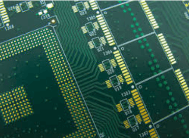
Hdi pcb 2+n+2
Advantages Of HDI PCB 2+N+2 In Modern Electronics
High-Density Interconnect (HDI) Printed Circuit Boards (PCBs) have become a cornerstone in the advancement of modern electronics, offering numerous advantages that cater to the ever-evolving demands of technology.
Among the various configurations of HDI PCBs, the 2+N+2 structure stands out for its unique benefits, making it a preferred choice in the design and manufacturing of sophisticated electronic devices. This configuration, characterized by two high-density outer layers and multiple inner layers, provides a robust platform for integrating complex circuitry in a compact form.
One of the primary advantages of HDI PCB 2+N+2 is its ability to support miniaturization without compromising performance.
As electronic devices continue to shrink in size, the need for compact yet powerful components becomes increasingly critical. The 2+N+2 configuration allows for a higher density of components and interconnections, enabling designers to pack more functionality into smaller spaces. This is particularly beneficial in the development of portable devices such as smartphones, tablets, and wearable technology, where space is at a premium.
In addition to facilitating miniaturization, HDI PCB 2+N+2 enhances signal integrity and performance.
The configuration’s design minimizes the length of signal paths, reducing the potential for signal loss and electromagnetic interference. This is crucial in high-speed applications where maintaining signal quality is paramount. Furthermore, the use of microvias in HDI PCBs allows for more efficient routing of signals between layers, contributing to improved electrical performance. As a result, devices utilizing HDI PCB 2+N+2 can achieve faster processing speeds and greater reliability, which are essential attributes in today’s competitive electronics market.
Moreover, the 2+N+2 structure offers significant design flexibility, allowing engineers to implement complex circuit designs with ease.
The additional layers provide ample space for routing intricate circuits, accommodating a wide range of design requirements. This flexibility is particularly advantageous in the development of advanced technologies such as 5G communication systems, automotive electronics, and medical devices, where intricate circuitry is often necessary to meet specific functional and regulatory standards.
Another notable advantage of HDI PCB 2+N+2 is its contribution to thermal management.
As electronic devices become more powerful, they generate more heat, which can adversely affect performance and longevity. The multilayer design of the 2+N+2 configuration facilitates efficient heat dissipation, helping to maintain optimal operating temperatures. This is achieved through the strategic placement of thermal vias and the use of materials with high thermal conductivity, ensuring that heat is effectively distributed away from critical components.
In conclusion, the HDI PCB 2+N+2 configuration offers a multitude of advantages that are instrumental in the advancement of modern electronics. Its ability to support miniaturization, enhance signal integrity, provide design flexibility, and improve thermal management makes it an invaluable asset in the development of cutting-edge technologies. As the demand for more compact, efficient, and powerful electronic devices continues to grow, the role of HDI PCB 2+N+2 in meeting these challenges is likely to become even more pronounced, solidifying its position as a key enabler of innovation in the electronics industry.
Design Considerations For HDI PCB 2+N+2 Layouts
In the realm of modern electronics, High-Density Interconnect (HDI) printed circuit boards (PCBs) have emerged as a pivotal technology, enabling the miniaturization and enhanced performance of electronic devices. Among the various configurations of HDI PCBs, the 2+N+2 layout stands out for its ability to balance complexity and functionality. This configuration, characterized by two microvia layers on both the top and bottom of the board, sandwiching N layers of traditional circuitry, offers a unique set of design considerations that engineers must meticulously address to ensure optimal performance and manufacturability.
To begin with, one of the primary considerations in designing HDI PCB 2+N+2 layouts is the selection of materials.
The choice of substrate material is crucial, as it must support the high-density interconnections while maintaining mechanical stability and thermal reliability. Materials with low dielectric constants and high glass transition temperatures are often preferred, as they minimize signal loss and withstand the thermal stresses encountered during manufacturing and operation. Furthermore, the compatibility of these materials with the microvia drilling process, typically laser drilling, is essential to ensure precise and reliable interconnections.
Transitioning to the aspect of signal integrity, the 2+N+2 configuration necessitates careful planning of the signal routing to mitigate issues such as crosstalk and electromagnetic interference (EMI).
The proximity of multiple layers in this configuration can exacerbate these issues if not properly managed. Therefore, designers must employ strategies such as controlled impedance routing, differential pair routing, and the use of ground planes to shield sensitive signals. Additionally, the placement of decoupling capacitors close to power pins can help stabilize power delivery and reduce noise, further enhancing signal integrity.
Another critical consideration is the thermal management of the HDI PCB 2+N+2 layout.
As electronic devices become more compact and powerful, the heat generated by densely packed components can pose significant challenges. Effective thermal management strategies, such as the incorporation of thermal vias, heat sinks, and thermal interface materials, are essential to dissipate heat efficiently and prevent overheating. Moreover, the layout should facilitate even heat distribution across the board to avoid hotspots that could compromise the reliability of the device.
In addition to these technical considerations, manufacturability is a key factor in the design of HDI PCB 2+N+2 layouts.
The complexity of this configuration demands precise manufacturing processes, including advanced drilling and plating techniques. Designers must collaborate closely with manufacturers to ensure that the design is not only feasible but also cost-effective to produce. This collaboration often involves iterative design reviews and adjustments to align with the capabilities and limitations of the manufacturing process.
Finally, testing and validation are indispensable steps in the design process of HDI PCB 2+N+2 layouts.
Rigorous testing protocols, including electrical testing, thermal cycling, and reliability assessments, are necessary to verify that the board meets the required performance standards. These tests help identify potential issues early in the development cycle, allowing for timely modifications and ensuring that the final product is robust and reliable.
In conclusion, the design of HDI PCB 2+N+2 layouts is a complex endeavor that requires careful consideration of materials, signal integrity, thermal management, manufacturability, and testing. By addressing these factors comprehensively, engineers can harness the full potential of this advanced configuration, paving the way for the next generation of high-performance electronic device
Manufacturing Challenges In HDI PCB 2+N+2 Production
The production of High-Density Interconnect (HDI) Printed Circuit Boards (PCBs) has become increasingly significant in the electronics industry, particularly with the advent of the 2+N+2 structure. This configuration, characterized by two outer layers and multiple inner layers, offers enhanced performance and miniaturization capabilities. However, the manufacturing of HDI PCBs with a 2+N+2 structure presents several challenges that manufacturers must navigate to ensure quality and efficiency.
To begin with, the complexity of the 2+N+2 structure necessitates precise fabrication techniques.
The intricate design requires advanced laser drilling technology to create microvias, which are essential for interlayer connections. These microvias must be accurately positioned and drilled to maintain the integrity of the electrical pathways. Any deviation in the drilling process can lead to defects, such as misalignment or incomplete vias, which can compromise the functionality of the PCB. Therefore, manufacturers must invest in state-of-the-art equipment and skilled personnel to achieve the necessary precision.
Moreover, the lamination process in HDI PCB production is another area fraught with challenges.
The 2+N+2 structure involves multiple lamination cycles to build the layers, which increases the risk of defects such as delamination and warping. These issues can arise from improper temperature control or pressure application during the lamination process. Consequently, manufacturers must implement stringent process controls and monitoring systems to ensure that each lamination cycle is executed flawlessly. This includes maintaining optimal environmental conditions and using high-quality materials that can withstand the rigors of repeated lamination.
In addition to these technical challenges, the production of HDI PCBs with a 2+N+2 structure also involves significant cost considerations.
The advanced equipment and materials required for this type of PCB are often more expensive than those used in traditional PCB manufacturing. Furthermore, the need for highly skilled technicians and engineers to oversee the production process adds to the overall cost. As a result, manufacturers must carefully balance the need for quality and performance with cost-effectiveness. This often involves optimizing production processes to reduce waste and improve yield, as well as exploring alternative materials that offer similar performance at a lower cost.
Furthermore, the testing and quality assurance phase in HDI PCB production is critical to ensuring that the final product meets the required standards.
Given the complexity of the 2+N+2 structure, traditional testing methods may not be sufficient to detect all potential defects. Advanced testing techniques, such as automated optical inspection and X-ray inspection, are often necessary to thoroughly evaluate the integrity of the PCB. These methods allow for the detection of hidden defects that could affect the performance and reliability of the final product. Therefore, manufacturers must invest in comprehensive testing protocols to ensure that each PCB meets the stringent requirements of modern electronic devices.
In conclusion, while the production of HDI PCBs with a 2+N+2 structure offers significant advantages in terms of performance and miniaturization, it also presents a range of manufacturing challenges. From the precision required in drilling microvias to the complexities of the lamination process, manufacturers must navigate a host of technical and cost-related issues. By investing in advanced technology, skilled personnel, and rigorous quality assurance processes, manufacturers can overcome these challenges and produce high-quality HDI PCBs that meet the demands of today’s electronics industry.
Applications Of HDI PCB 2+N+2 In Consumer Electronics
High-Density Interconnect (HDI) Printed Circuit Boards (PCBs) have become a cornerstone in the advancement of consumer electronics, particularly the 2+N+2 configuration. This specific configuration refers to a multilayer PCB structure with two high-density outer layers and N number of standard inner layers, flanked by two additional high-density layers. The 2+N+2 HDI PCB design is renowned for its ability to support complex circuitry in a compact form, making it an ideal choice for modern consumer electronics that demand both performance and miniaturization.
One of the primary applications of HDI PCB 2+N+2 in consumer electronics is in smartphones.
As smartphones continue to evolve, there is a constant push for more features, better performance, and longer battery life, all within a sleek and compact design. The 2+N+2 configuration allows for a higher component density, enabling manufacturers to integrate more functionalities without increasing the size of the device. This is achieved through the use of microvias, blind vias, and buried vias, which facilitate the interconnection of multiple layers, thereby optimizing the available space on the PCB. Consequently, this leads to enhanced processing power and improved energy efficiency, which are critical for the seamless operation of smartphones.
In addition to smartphones, HDI PCB 2+N+2 is extensively used in tablets and laptops.
These devices require a delicate balance between performance and portability, a challenge that the 2+N+2 configuration adeptly addresses. By allowing for a more compact design, these PCBs enable the production of thinner and lighter devices without compromising on functionality. The increased interconnect density supports advanced features such as high-resolution displays, faster processors, and extended battery life, all of which are essential for meeting consumer expectations in a competitive market.
Wearable technology is another domain where HDI PCB 2+N+2 plays a pivotal role.
Devices such as smartwatches and fitness trackers demand a high level of integration in a very limited space. The 2+N+2 configuration provides the necessary framework to incorporate sensors, processors, and communication modules within a small footprint. This not only enhances the functionality of wearables but also contributes to their aesthetic appeal by allowing for sleek and stylish designs. Moreover, the reliability and durability of HDI PCBs ensure that these devices can withstand the rigors of daily use.
Furthermore, the application of HDI PCB 2+N+2 extends to the realm of home automation and smart appliances.
As the Internet of Things (IoT) continues to expand, there is an increasing demand for interconnected devices that can communicate seamlessly. The 2+N+2 configuration supports the integration of wireless communication modules and sensors, enabling smart devices to interact with each other and with users efficiently. This facilitates the development of intelligent home systems that enhance convenience, security, and energy management.
In conclusion, the HDI PCB 2+N+2 configuration is instrumental in the advancement of consumer electronics, offering a solution that meets the demands for miniaturization, performance, and reliability. Its application across various devices, from smartphones to smart home systems, underscores its versatility and importance in the ever-evolving landscape of consumer technology. As the demand for more sophisticated and compact electronic devices continues to grow, the role of HDI PCB 2+N+2 is likely to become even more significant, driving innovation and shaping the future of consumer electronics.