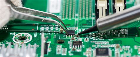
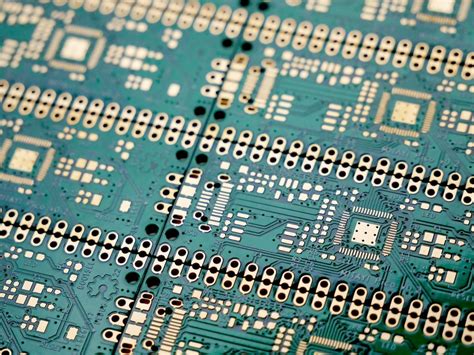
Hdi pcb application
Enhancing Signal Integrity in HDI PCB Applications
High-Density Interconnect (HDI) printed circuit boards (PCBs) have become a cornerstone in the advancement of modern electronics, primarily due to their ability to enhance signal integrity. As electronic devices continue to shrink in size while increasing in functionality, the demand for PCBs that can support higher component densities and finer lines has surged. HDI PCBs, with their intricate design and advanced manufacturing processes, offer a solution that not only meets these demands but also significantly improves signal integrity, a critical factor in the performance of electronic devices.
Signal integrity refers to the preservation of the quality of electrical signals as they travel through a circuit.
In HDI PCBs, maintaining signal integrity is paramount, especially as the complexity and speed of electronic devices increase. One of the primary ways HDI PCBs enhance signal integrity is through the use of microvias. These are small vias that connect different layers of a PCB, allowing for shorter and more direct signal paths. By minimizing the distance that signals must travel, microvias reduce the potential for signal loss and distortion, thereby improving overall signal quality.
Moreover, HDI PCBs often incorporate multiple layers, which allow for better separation of signal and power planes.
This separation is crucial in minimizing electromagnetic interference (EMI), a common issue that can degrade signal integrity. By strategically placing ground and power planes between signal layers, HDI PCBs can effectively shield sensitive signals from external noise, thus preserving their integrity. Additionally, the use of advanced materials with low dielectric constants in HDI PCBs further aids in reducing signal loss and enhancing performance.
Another significant advantage of HDI PCBs in enhancing signal integrity is their ability to support higher data rates.
As the demand for faster data transmission continues to grow, HDI PCBs provide the necessary infrastructure to accommodate these requirements. The fine lines and spaces in HDI PCBs allow for the routing of high-speed signals with minimal crosstalk, a phenomenon where a signal transmitted on one circuit or channel creates an undesired effect on another circuit or channel. By reducing crosstalk, HDI PCBs ensure that high-speed signals maintain their integrity, which is essential for the reliable operation of modern electronic devices.
Furthermore, the compact design of HDI PCBs contributes to improved thermal management, which indirectly supports signal integrity.
As electronic components become more densely packed, managing heat dissipation becomes increasingly challenging. HDI PCBs, with their efficient use of space and materials, facilitate better heat distribution, thereby reducing the risk of overheating. This thermal stability is crucial, as excessive heat can lead to signal degradation and component failure.
In conclusion, HDI PCBs play a pivotal role in enhancing signal integrity in modern electronic applications.
Through the use of microvias, multilayer designs, advanced materials, and efficient thermal management, HDI PCBs address the challenges posed by increased component density and higher data rates. As technology continues to evolve, the importance of maintaining signal integrity will only grow, making HDI PCBs an indispensable component in the development of next-generation electronic devices. By ensuring that signals are transmitted accurately and reliably, HDI PCBs not only enhance device performance but also pave the way for future innovations in the electronics industry.
Miniaturization Trends: The Role of HDI PCBs in Modern Electronics
In the rapidly evolving landscape of modern electronics, the demand for smaller, more efficient devices has never been greater. This trend towards miniaturization is driven by consumer expectations for portable, high-performance gadgets, as well as the technological advancements that make such innovations possible. At the heart of this miniaturization movement lies the High-Density Interconnect (HDI) printed circuit board (PCB), a pivotal component that enables the creation of compact, yet powerful electronic devices.
HDI PCBs are characterized by their higher wiring density per unit area compared to traditional PCBs.
This is achieved through the use of finer lines and spaces, smaller vias, and capture pads, as well as higher connection pad density. These features allow for more components to be placed on both sides of the board, significantly reducing the overall size of the electronic device. Consequently, HDI technology is instrumental in the development of modern electronics, where space is at a premium.
One of the primary applications of HDI PCBs is in the smartphone industry.
As consumers demand more features and better performance from their mobile devices, manufacturers are compelled to incorporate more functionality into a limited space. HDI PCBs facilitate this by allowing for the integration of multiple functions into a single, compact board. This not only reduces the size of the device but also enhances its performance and reliability. Moreover, the use of HDI technology in smartphones supports the inclusion of advanced features such as high-resolution cameras, faster processors, and larger memory capacities, all while maintaining a sleek and lightweight design.
In addition to smartphones, HDI PCBs are also crucial in the production of other portable electronics, such as tablets, laptops, and wearable devices.
These products benefit from the same miniaturization advantages, enabling manufacturers to offer powerful computing capabilities in a portable form factor. Furthermore, the automotive industry is increasingly adopting HDI technology to support the growing complexity of electronic systems in modern vehicles. From advanced driver-assistance systems (ADAS) to infotainment and connectivity solutions, HDI PCBs provide the necessary platform for integrating sophisticated electronic components within the limited space available in vehicles.
The medical field is another area where HDI PCBs are making a significant impact.
Medical devices, such as implantable devices, diagnostic equipment, and portable monitoring systems, require compact and reliable electronic solutions. HDI technology allows for the miniaturization of these devices, making them less invasive and more comfortable for patients, while also enhancing their functionality and performance.
As the demand for smaller, more efficient electronic devices continues to grow, the role of HDI PCBs in facilitating this trend becomes increasingly important. The ability to pack more functionality into a smaller space not only meets consumer expectations but also drives innovation across various industries. In conclusion, HDI PCBs are a cornerstone of modern electronics, enabling the miniaturization of devices without compromising on performance or reliability. As technology continues to advance, the significance of HDI technology in shaping the future of electronics will undoubtedly expand, paving the way for even more groundbreaking developments in the years to come.
Design Challenges and Solutions in HDI PCB Applications
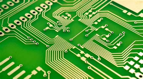
High-Density Interconnect (HDI) printed circuit boards (PCBs) have become a cornerstone in the advancement of modern electronics, offering significant benefits such as reduced size, increased functionality, and enhanced performance. However, the design and implementation of HDI PCBs present a unique set of challenges that require innovative solutions to overcome. Understanding these challenges and their corresponding solutions is crucial for engineers and designers aiming to leverage the full potential of HDI technology.
One of the primary challenges in HDI PCB design is managing the increased complexity that comes with higher component density.
As devices become more compact, the need to fit more components into a smaller area becomes imperative. This often leads to intricate routing and the necessity for multiple layers, which can complicate the design process. To address this, designers employ advanced computer-aided design (CAD) tools that facilitate precise layout planning and simulation. These tools allow for the optimization of trace routing and layer stacking, ensuring that the design meets both electrical and mechanical requirements.
In addition to complexity, thermal management poses a significant challenge in HDI PCB applications.
The compact nature of these boards can lead to heat accumulation, which, if not properly managed, can affect the performance and reliability of the device. To mitigate this issue, designers incorporate thermal vias and heat sinks into the PCB design. These elements help dissipate heat away from critical components, maintaining optimal operating temperatures. Furthermore, selecting materials with high thermal conductivity for the PCB substrate can enhance heat dissipation, thereby improving the overall thermal performance of the board.
Signal integrity is another critical concern in HDI PCB design.
As the frequency of operation increases, the risk of signal degradation due to crosstalk, electromagnetic interference (EMI), and impedance mismatches also rises. To combat these issues, designers must carefully consider the placement of components and the routing of traces. Utilizing differential signaling and controlled impedance traces can significantly reduce the impact of these factors. Additionally, incorporating ground planes and shielding techniques can further enhance signal integrity by minimizing EMI and crosstalk.
The manufacturing process of HDI PCBs also presents its own set of challenges.
The precision required for microvias and fine lines necessitates advanced fabrication techniques, which can increase production costs and time. To address these challenges, manufacturers have developed innovative processes such as laser drilling for microvias and the use of advanced photolithography for fine line etching. These techniques not only improve the accuracy and reliability of the manufacturing process but also enable the production of more complex HDI designs.
Finally, the testing and validation of HDI PCBs require specialized equipment and methodologies.
Due to the high density and complexity of these boards, traditional testing methods may not be sufficient. Advanced testing techniques, such as automated optical inspection (AOI) and X-ray inspection, are employed to ensure the integrity and functionality of the final product. These methods allow for the detection of defects that may not be visible through conventional inspection techniques, thereby ensuring the reliability of the HDI PCB.
In conclusion, while HDI PCB applications present several design challenges, the development of innovative solutions and advanced technologies has enabled designers and manufacturers to overcome these obstacles. By addressing complexity, thermal management, signal integrity, manufacturing precision, and testing requirements, the industry continues to push the boundaries of what is possible with HDI technology, paving the way for more compact, efficient, and powerful electronic devices.
HDI PCBs in Automotive Electronics: Driving Innovation
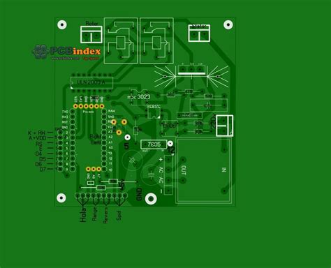
High-Density Interconnect (HDI) printed circuit boards (PCBs) have emerged as a pivotal technology in the realm of automotive electronics, driving innovation and enabling the development of more sophisticated, efficient, and reliable vehicle systems. As the automotive industry continues to evolve, the demand for advanced electronic systems has surged, necessitating the integration of more complex circuitry within limited spaces. HDI PCBs, with their compact design and enhanced performance capabilities, have become instrumental in meeting these demands.
One of the primary advantages of HDI PCBs in automotive applications is their ability to support miniaturization.
Modern vehicles are equipped with a multitude of electronic components, ranging from infotainment systems and advanced driver-assistance systems (ADAS) to engine control units and sensors. These components require PCBs that can accommodate high component density without compromising performance. HDI PCBs, characterized by their finer lines and spaces, smaller vias, and higher connection pad density, allow for the integration of more components in a smaller area. This miniaturization not only saves space but also reduces the overall weight of the vehicle, contributing to improved fuel efficiency and reduced emissions.
Moreover, HDI PCBs enhance the performance and reliability of automotive electronic systems.
The use of microvias and blind/buried vias in HDI technology facilitates shorter signal paths, which in turn reduces signal loss and improves signal integrity. This is particularly crucial in automotive applications where precise and reliable data transmission is essential for the proper functioning of safety-critical systems such as ADAS and electronic stability control. Additionally, the improved thermal management capabilities of HDI PCBs help in dissipating heat more effectively, thereby enhancing the longevity and reliability of electronic components in the harsh automotive environment.
Transitioning to the aspect of design flexibility, HDI PCBs offer significant advantages.
The ability to incorporate multiple layers and advanced interconnect techniques allows designers to create more complex and customized circuit layouts. This flexibility is vital in the automotive sector, where electronic systems must be tailored to meet specific performance and safety requirements. For instance, the integration of HDI PCBs in electric vehicles (EVs) supports the development of more efficient battery management systems and power electronics, which are crucial for optimizing energy consumption and extending the driving range of EVs.
Furthermore, the adoption of HDI PCBs aligns with the automotive industry’s shift towards greater connectivity and automation.
As vehicles become increasingly connected, the need for robust and high-speed data communication networks within the vehicle architecture becomes paramount. HDI PCBs, with their ability to support high-frequency signals and high-speed data transmission, are well-suited to meet these requirements. This capability is essential for enabling seamless communication between various electronic control units and ensuring the smooth operation of connected and autonomous vehicle technologies.
In conclusion, HDI PCBs are driving innovation in automotive electronics by enabling the development of more compact, efficient, and reliable systems. Their role in supporting miniaturization, enhancing performance, offering design flexibility, and facilitating connectivity is crucial as the automotive industry continues to advance towards more sophisticated and sustainable vehicle technologies. As such, the integration of HDI PCBs is set to play an increasingly important role in shaping the future of automotive electronics, paving the way for safer, smarter, and more efficient vehicles.

