How to Design a PCB or Other Circuit Board: The Basics
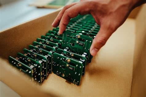
In the world of electronics, PCBs or circuit boards are the most integral part of any electronic device. They are often overlooked as they are hidden underneath the housing of the electronic device, but they are really the backbone of any device, electronic gadget, and device you own. A PCB (Printed Circuit Board) houses all the electronic components of a device and are electrically connected to each other to create a circuit. It is designed to hold all the wires and other components in place, as it is reasonable.
If you are into electronics manufacturing, it is no surprise that if you want to know how to design a PCB board, and you want to know the PCB design steps the most. Even though you can always buy ready-made circuit boards, it will be too expensive if you are just a small electronics business. As a small-scale electronics manufacturer, it is absolutely necessary to do it yourself.
There are 3 different methods for designing circuit boards.
Handmade Circuit Iron on Glossy Paper Laser Cutting Method The laser cutting method is the top technique used in the industry when creating printed circuit board designs. It requires laser machinery, which is too expensive for small and even medium-sized businesses. In this wiki article, let us focus on the other two methods of how to design PCB boards: Handmade Circuit and Iron on Glossy Paper.
A step by step process on how to design a PCB (Circuit Board) First you need to think of the schematic of your circuit before you think of mounting it on the board.
Luckily there are already many free software that can handle PCB layout design. Some of them are paid packages that give an in-depth look at PCB layout design and whether you choose free or paid will be up to you.
Once you have your PCB layout design ready, now you have to secure the materials you will need as part of the PCB design guidelines.
Here are the materials you will need; Copper Plate Etching Liquid Glossy Paper Black Marker Cutter Sandpaper Kitchen Paper Cotton Wool Steel Wool For an example on how to design a circuit board, let us consider a PCB design for a simple touch switch device using IC555.
- Print out the board layout.
Print the board layout using glossy paper and make sure you print on the glossy side of the paper. Select black output from the PCB design layout and printer settings.
- Cut the copper plate of the PCB.
Cut the copper plate as per the appropriate size for your PCB layout. The smaller the board, the better for the overall effect as we want to keep the size minimal and minimized but at the same time keep room for all the electrical components.
Wipe the copper side of the PCB with steel wool to remove the copper oxide layer as well as the photoresist surface. Having a smooth surface allows the image of the printout to adhere better.
- Transfer the printout to the copper board.
Transfer the printout by placing it on the copper surface of the PCB and make sure the board is properly aligned on the border. Tape the printout to the board if necessary to hold it in the correct position.
Next, it’s a two-way street here as the two different methods mentioned above about designing a PCB board will come into play.
a. Handcrafting a circuit reference When tracing the layout of the board on the copper board with a pencil. Once you are happy with the sketch, trace it again with a permanent black marker.
b. Iron on Glossy Paper This is another method where you iron the glossy paper of the printout face down to the copper side of the plate. Simply place the glossy paper on the copper board with the back of the glossy paper on the surface. Hold the glossy paper and copper board in place with pliers and place a flat iron on the other end for 8-10 seconds. Repeat the process for the other surfaces, moving them around on the pliers to keep them in place.
Once the entire surface of the glossy paper has been covered, iron the glossy paper along the edges for 10 to 15 minutes with a little pressure. This ironing process transfers the ink to the copper plate due to the heat. Be careful with the hot surface of the copper plate due to the hot iron.
After ironing, place the copper plate in warm water for 10 minutes. The paper will dissolve immediately, allowing you to peel it off easily. However, sometimes the ink will darken after peeling, but you can easily fix it by going over the ink again with a black marker.
- Etch the board.
This is arguably the most critical step in making a PCB: the etching process. You have to be very careful during this process, first wear sanitary gloves for protection. Put some paper on the bottom end so that the etching solution does not leave marks on the floor. Meanwhile, fill a plastic box with water and dissolve 2-3 teaspoons of etching solution (usually ferric chloride) in the water.
Immerse the PCB in the solution and leave it for half an hour. The etching solution will react with the copper surface, removing the copper from the PCB without any traces on it. If it is not etched correctly, leave the board in the solution for a few more minutes. Remove the useless copper with pliers.
- Clean the PCB and make the final touches.
The etching solution is highly toxic and you must dispose of it correctly. Do not simply drain it down the sink as it can damage your pipes. Instead, dilute the solution with more water and throw it somewhere outside the house.
To remove residual ink from the PCB, a few drops of the thinner on a piece of cotton board will do the job. Simply rub it on the surface, then rinse it carefully with water and dry it with a cloth or kitchen paper. Trim the board to the desired size and smooth the edges by sandpaper.
For the final step, use a PCB drill to drill holes on the printed circuit board design. Use a soldering iron to attach all the cool components to the board. Apply solder mask on some PCB paint if you want to use a traditional green printed circuit board design.
Follow these PCB design guidelines carefully and now you can have a cost-effective DIY PCB or circuit board. The housing of the PCB usually starts with a 3D design and then continues with plastic manufacturing.