What is a printed circuit board? What are the functions of a printed circuit board?
Printed circuit boards (PCBs) are convenient thin sheets used to house interconnected electrical components in a simple, convenient and economical manner. They are used as a physical support for mounting and connecting different electrical components.
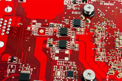
PCBs are made of fiberglass, composite epoxy or any other composite material with a metal coated surface.
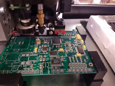
They have an etching made using metal and acid to create the circuits that go through different integrated circuits (ICs) and other components on the board. Solder connects the ICs and other components to the surface of the board. The copper tracks in the circuit board reduce the possibility of short circuits, misaligned or misplaced wires.
In this way, all components are firmly fixed to the board without the need for complex wiring systems and unnecessary expenses.
This also simplifies the process of maintaining the PCB according to your needs – there is no need to deal with a lot of wires.
However, not all electrical applications use standard PCBs. In fact, they vary according to the size, shape and function of the electronic device. For example, the type of PCB used in a smartwatch is different from the type of PCB used in a TV.
Designing a complex circuit is one aspect of the challenge, and translating the circuit design into a PCB design is another aspect.
This design must be well translated into a physical form so that the desired circuit is formed. A perfect PCB design is always the key to success in the manufacturing process, while a poorly designed PCB leads to wasted time and effort, rework, and product failure. Worse still, it may end up being useless and the results are not relevant to real-world scenarios.
Therefore, a PCB designer must have a good knowledge of the manufacturing process in addition to the knowledge of positioning hundreds of components and traces that meet physical and electrical requirements.
PCB designers must follow the Design for Assembly (DFA) related standards when designing PCBs.
These standards refer to the cost and efficiency of the product and provide the lowest risk, clarity, and simplification. Even assembler capabilities are important to get the overall picture of DFA.
Substrate material fr4 is usually used to create normal and complex PCB designs, while polyamide material is used for high-speed RF capable designs. When deciding on the choice of substrate material, designers must have a deep understanding of the environmental conditions that the PCB assembly can withstand.
Complex PCB designs may have some special assembly requirements such as mechanical component assembly, press fittings, adhesives, wire harnesses, housing components, wire harnesses, and test points. Therefore, designers must consider all these factors so that they can organize the placement details of components accordingly.
Complex PCB designs require some additional complex processes, including via-in-pad, wire soldering, wave soldering, on-board IC programming, conformal coating, surface treatment, etc. These requirements are not applicable to general PCB designs.
The design concepts are the same for all PCB design processes, but they are different for high-speed RF capabilities because these designs must consider resistance, inductance and capacitance, as well as traces and dielectrics that affect the signal increase times and impedance, thereby limiting the upper frequency.
Similarly, PCB design rules for wave soldering processes are different in the design of component orientation and pad shape
. Getting the right pad shape is the main concern for fine pitch surface mount parts, while shadowing is the main concern for part positioning.
The reason for the creation of double-sided printed circuit boards is because the placement of complex components such as BGA, CSP, QFP, DFN POP on the top will not directly contact the wave. If it is unavoidable, then the package should be rotated 45 degrees relative to the propagation direction of the wave.
Standards and specifications for PCB design performance and accessibility include IPC-2221, ipc-6011 and IPC-6012.
Many PCB design software applications (PCB layout SW) are available as Windows-based software packages, such as CAD SOFT, Eagle PCB, Novarm’s DipTrace, etc.
Benefiting from the transfer of global PCB production capacity to the mainland and the booming downstream electronic terminal product manufacturing, the overall PCB market in mainland China has shown a rapid development trend. From 2014 to 2019, the scale of PCB output value in mainland China has generally shown a steady upward trend. Since 2019, Sino-US economic and trade frictions have intensified, economic uncertainty has increased, and the PCB industry has fluctuated in the short term, but the medium- and long-term growth trend is still relatively certain. According to Prismark, by 2025, the overall scale of China’s PCB industry market will grow to US$42 billion.
PCB has the following functions in electronic devices.
(1) Provide mechanical support for fixing and assembling various electronic components such as integrated circuits, realize wiring and electrical connection or electrical insulation between various electronic components such as integrated circuits, and provide the required electrical characteristics.
(2) Provide solder mask patterns for automatic welding, and provide identification characters and patterns for component insertion, inspection, and maintenance.
(3) After electronic equipment uses printed circuit boards, due to the consistency of similar printed circuit boards, manual wiring errors are avoided, and electronic components can be automatically inserted or mounted, automatically soldered, and automatically inspected, ensuring the quality of electronic products, improving labor productivity, reducing costs, and facilitating maintenance.
(4) Provide the required electrical characteristics, characteristic impedance, and electromagnetic compatibility characteristics for circuits in high-speed or high-frequency circuits.
(5) Printed circuit boards with passive components embedded inside provide certain electrical functions, simplify electronic installation procedures, and improve product reliability.
(6) In large-scale and ultra-large-scale electronic packaging components, it provides an effective chip carrier for miniaturized chip packaging of electronic components.