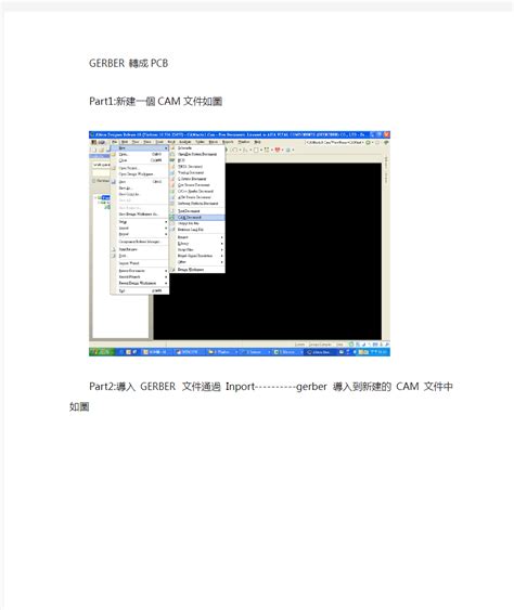
Converting Gerber Files to PCB Designs Made Easy
Key Takeaways
In the journey of transforming Gerber files into effective PCB designs, several key insights can significantly enhance your approach. First, having a solid understanding of what Gerber files entail is essential. These files serve as the universal standard for PCB manufacturing, detailing various elements like copper layers, silkscreen, and solder masks. When preparing to engage with PCB manufacturing companies, be aware that the choice of tools can greatly influence your efficiency and accuracy. Selecting the right software for conversion is crucial; it can streamline your workflow and minimize errors during PCB manufacturing.
Moreover, it is important to acknowledge the potential challenges that may arise during this conversion process. However, by employing proven strategies, you can overcome these hurdles effectively—ensuring that your PCB manufacturing cost remains within budget while maintaining high standards in design accuracy. Optimizing your workflow not only saves time but also enhances productivity in your PCB manufacturing business. Thus, as you venture into converting Gerber files to PCB designs, keep these key takeaways in mind to ensure a smooth and successful transition. These insights will empower you as you start your next project with confidence.
Understanding Gerber Files: A Brief Overview
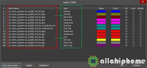
When embarking on your journey in PCB manufacturing, it’s essential to grasp the concept of Gerber files. These files act as the blueprint for your circuit boards, providing the necessary details to ensure your design is accurately translated into a physical product. Essentially, Gerber files contain a plethora of information, including the copper layers, silkscreen layers, and solder mask data. Understanding how these files work ensures that you can effectively communicate with PCB manufacturing companies, allowing for seamless production.
Gerber files are typically generated from your PCB design software and come in various formats; however, the most common standard is RS-274X. When you need to convert these files into an actionable format for PCB manufacturing, you might face challenges, particularly if the nuances of your design are not preserved through conversion processes.
To give you an idea of how crucial Gerber files are in determining PCB manufacturing cost, consider a comparative table showcasing different types of file outputs and their efficacy:
| File Type | Description | Accuracy Level | Cost Impact |
|---|---|---|---|
| RS-274X | Standard Gerber format | High | Moderate |
| ODB++ | Advanced package with metadata | Very High | High |
| IPC-2581 | XML-based standard format | Medium | Varies widely |
By recognizing the importance of maintaining high accuracy during these conversions, you can significantly reduce errors leading to increased costs associated with rework. This understanding allows you to streamline your workflow when working with PCB manufacturing businesses and ensure that every aspect of your design is accounted for.
Navigating through the intricacies of Gerber files not only enhances your technical proficiency but also sets a strong foundation for successful PCB projects. By mastering this aspect early on, you will be well-prepared to tackle more complex challenges in your future endeavors within the realm of PCB manufacturing.
Tools and Software Needed for Conversion
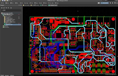
When converting Gerber files to PCB designs, having the right tools and software is crucial for ensuring a smooth and efficient process. Opt for specialized PCB design software that supports importing Gerber files. Popular options include Altium Designer, KiCad, and Eagle, each offering various functionalities that cater to different needs.
While selecting your tools, consider the PCB manufacturing companies you plan to work with, as some may have preferred formats or specific requirements for the files they accept. This consideration can help minimize manufacturing costs and streamline your workflow.
Furthermore, utilizing viewer applications can help you analyze Gerber files before conversion. This step is crucial in identifying any potential issues that might arise during the conversion process. For instance, a viewer can help you verify that all layers are correctly represented and that there are no discrepancies in your design.
“The right tool not only improves efficiency but also enhances the accuracy of your PCB layout,” so investing in appropriate software is paramount.
Remember to keep an eye on any emerging tools or updates from PCB manufacturing companies that could provide better options or features suited to your needs. As technology evolves, so does the capability of these tools, which could further reduce PCB manufacturing costs while enhancing quality. By equipping yourself with the best resources in your conversion journey, you’ll be well on your way to creating successful PCB projects efficiently.
Step-by-Step Guide to Converting Gerber to PCB
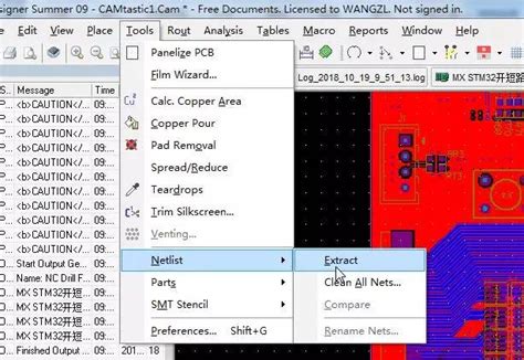
Converting Gerber files to PCB designs can appear daunting, but with the right approach, you can simplify the process. Start by understanding that Gerber files are the industry standard for PCB manufacturing, containing precise information about circuit layouts. Your first step is selecting the appropriate software; many tools are available that facilitate the conversion seamlessly. These applications often allow you to import your Gerber files, making it easier to visualize and edit your PCB design.
Once imported, ensure that all layers are properly aligned and that there’s a clear understanding of the different component layers such as solder mask, silkscreen, and copper layers. This step is crucial because inaccuracies in layer alignment can lead to costly mistakes in your PCB manufacturing. As you refine your design, keep a close eye on potential oversights in design rules compared to industry standards set by various PCB manufacturing companies.
Incorporating this understanding of layout rules not only enhances your design’s integrity but also helps control PCB manufacturing cost, an essential factor when considering bulk production for your PCB manufacturing business. Engaging with community forums or seeking advice from experienced professionals can also be beneficial as they often share insights on overcoming common pitfalls encountered during this transition. Through careful attention and iteration, you will be well on your way to creating an efficient and precise PCB design from your original Gerber files.
Common Challenges and How to Overcome Them
When converting Gerber files to PCB designs, several challenges can arise that may hinder the effectiveness of the transition. One common issue is file compatibility. Different PCB manufacturing companies may utilize various software, which can sometimes result in discrepancies when importing Gerber files. To overcome this, ensure you’re using compatible tools and validate the files within your software before proceeding.
Another challenge is maintaining design accuracy throughout the conversion process. Sometimes, tiny deviations can occur when transferring data from Gerber to PCB layout software. To tackle this, you should employ rigorous design rule checks (DRC) in your PCB design software after conversion to catch any discrepancies early on.
Additionally, understanding PCB manufacturing costs can be a hurdle, especially if you’re new to the industry. It’s important to familiarize yourself with how complexities in the design affect pricing and lead times. Consulting with industry professionals or using resources from reputable PCB manufacturers can provide insights that aid in defining your PCB manufacturing business strategy while controlling costs effectively.
Lastly, consider that component placement and routing might not perfectly translate from Gerber files to PCB formats due to differences in how layouts are interpreted by various tools. A practical solution is iterating your designs and collaborating closely with your manufacturer to ensure alignment between your vision and their production capabilities. By addressing these challenges systematically, you can enhance both the quality of your design and the efficiency of your workflow, setting a strong foundation for successful PCB projects ahead.
For further information on streamlining these processes, visit Andwin PCBA.
Ensuring Accuracy in Your PCB Designs
Accuracy in PCB designs is crucial to the success of your project, especially when transitioning from Gerber files. One misalignment can lead to significant issues during the PCB manufacturing process, wasting both time and resources. Therefore, it’s essential to verify that your converted designs align perfectly with your initial specifications. Start by cross-referencing your Gerber files with the final output, checking for discrepancies in pad sizes, traces, and overall layout. Utilize software designed for PCB manufacturing to simulate and visualize the design before moving forward with production. This ensures you’re aware of any potential errors that could affect your PCB manufacturing cost, especially if you plan to collaborate with various PCB manufacturing companies. By adopting comprehensive verification techniques and utilizing available tools effectively, you can enhance the accuracy of your designs and contribute greatly to a successful PCB manufacturing business.
Tips for Streamlining Your Workflow
When converting Gerber files to PCB designs, optimizing your workflow is essential for achieving efficient and accurate results. Begin by organizing all your project files and ensuring that you have ready access to the necessary software. Many PCB manufacturing companies provide powerful tools that can enhance your productivity during this conversion process. Familiarize yourself with features such as batch processing and library management, which can significantly reduce the PCB manufacturing cost by minimizing errors and rework.
To further streamline your workflow, establish a consistent naming convention for your files. This tactic not only saves time but also enhances collaboration among team members, allowing everyone to track changes without confusion. Don’t overlook the importance of component selection; spending time upfront to choose the right materials and layouts will pay off in the long run. As you embark on this journey towards efficient PCB manufacturing, consider using templates tailored for various PCB types, enabling a smooth transition from the design phase to production.
Implementing effective feedback loops during the design review stage can also minimize setbacks. By regularly engaging with colleagues or using simulation tools, you can catch potential issues before they escalate into costly mistakes in your PCB manufacturing business. Adhering to these strategies will help you enhance not only your current project outcomes but also lay a foundation for more successful conversions in future endeavors.
Case Studies: Successful Gerber to PCB Conversions
Exploring real-world case studies of successful conversions from Gerber files to PCB designs reveals valuable insights into the pcb manufacturing process. These examples illustrate how different designers and engineers tackled their unique challenges, ultimately leading to effective solutions. For instance, one small electronics startup managed to significantly reduce their pcb manufacturing cost by implementing a robust conversion workflow. They utilized specialized tools for accurate file transformation, ensuring that the design met industry standards while minimizing errors. Another case involved a larger company that collaborated with skilled pcb manufacturing companies, enabling them to pivot quickly when facing unexpected design changes. The integration of efficient software for Gerber file handling not only streamlined their operations but also led to a noticeable increase in production efficiency. These instances show that by understanding the complexities of pcb manufacturing and adopting best practices from those who have succeeded, you can enhance your own projects and potentially grow your pcb manufacturing business into a profitable venture. Implementing lessons learned from these case studies can serve as an excellent foundation for optimizing your conversion processes, reinforcing the importance of precision and adaptability in PCB design workflows.
Finalizing Your PCB Design: Best Practices
As you conclude your PCB design process, it’s essential to take critical steps to ensure everything is in order before sending your files off to PCB manufacturing. Begin by conducting a thorough review of your design, checking for common errors such as unconnected traces, overlapping components, or incorrect footprints. Utilize PCB manufacturing companies that offer Design Rule Checks (DRC); these can significantly increase your confidence that the layout will function as intended. Additionally, merging best practices like employing a clear labeling system for traces and components will aid in communication with those involved in the PCB manufacturing business and could even help reduce production lead time.
Don’t forget to assess the PCB manufacturing cost—it can vary widely based on factors like material choice, layer count, and complexity of design. By optimizing these aspects during the finalization phase, you can potentially save money without sacrificing quality. Testing prototypes before mass production is another key practice; this will not only help in identifying flaws missteps but also provide valuable insights that can improve future designs. Remember that meticulous attention to detail during this stage could save you time and resources down the line—an investment well worth making in the realm of electronic design.
Conclusion
In summary, converting Gerber files to PCB designs is a crucial step in the workflow of any PCB manufacturing business. By following the comprehensive guide provided, you can enhance your efficiency and accuracy in creating printed circuit boards. Have you considered how the choice of PCB manufacturing companies impacts your project? When selecting a partner for production, it’s essential to evaluate their reputation and ability to meet your specific needs. Understanding the nuances of PCB manufacturing costs can further empower you to make informed decisions, ensuring that your budget aligns with your project’s requirements. With these insights, you are now better equipped to tackle any challenges that arise in the conversion process and confidently move forward in your ventures within the world of PCB design and manufacturing. This knowledge will not only aid in meeting project deadlines but also contribute to creating high-quality products that stand out in today’s competitive landscape. Start implementing these practices and watch how they transform your approach to PCB projects!
FAQs
What are Gerber files, and why are they important in PCB manufacturing?
Gerber files are the standard file format used for PCB design. They provide all the necessary instructions for manufacturing your circuit board, including layer information, dimensions, and drill holes. In pcb manufacturing, accurate Gerber files are crucial to ensure your designs are realized correctly.
How can I convert Gerber files to PCB designs?
To convert Gerber files to PCB designs, you’ll need specific software tools. With a step-by-step approach, you can import the Gerber files into a PCB design program. This allows you to visualize and adjust your layout as needed before sending it off to pcb manufacturing companies.
What challenges might I face during the conversion process?
Challenges involve potential inaccuracies in layout representation or missing information in your Gerber files. To overcome these issues, thorough validation of the pcb manufacturing cost, as well as double-checking your files before conversion, is essential.
How can I ensure accuracy in my PCB designs after conversion?
Review your converted design meticulously against the original specifications. Employ verification tools provided by most PCB design software to catch any discrepancies early on in the process.
What tips do you have for streamlining my workflow during PCB design?
Utilize templates for similar projects to save time and maintain consistency. Organizing your components effectively within your layout will enhance clarity and reduce errors in both the design phase and when communicating with pcb manufacturing business partners.
For added guidance on efficient processes within pcb manufacturing, please click here.