Analysis and design of ocb power supply systerm
Today, it is difficult to successfully design high-speed electronic systems without a thorough understanding of the chip, package structure, and PCB power supply system characteristics. In fact, in order to meet lower power supply voltage, faster signal switching speed, higher integration and many increasingly challenging requirements, many companies at the forefront of electronic design have to ensure power supply during the product design process. and signal integrity, a large amount of money, manpower and material resources have been invested in the analysis of the power supply system.
The analysis and design of power supply systems (PDS) are becoming increasingly important in the field of high-speed circuit design, especially in the computer, semiconductor, communications, networking, and consumer electronics industries. As VLSI technology inevitably shrinks further, the power supply voltage of integrated circuits will continue to decrease. As more and more manufacturers switch from 130nm technology to 90nm technology, it can be expected that the supply voltage will drop to 1.2v or even lower, while the current will also increase significantly. From the perspective of DC IR voltage drop to AC dynamic voltage fluctuation control, since the allowable noise range is getting smaller and smaller, this development trend has brought huge challenges to the design of power supply systems.
PCB power supply system design overview
Usually in AC analysis, the input impedance between the power supply ground is an important observation to measure the characteristics of the power supply system. The determination of this observation quantity evolves into the calculation of ir voltage drop in DC analysis. No matter in the analysis of DC or AC, the factors that affect the characteristics of the power supply system include: the layering of the PCB, the shape of the power board plane, the layout of the components, the distribution of vias and pins, etc.
The concept of input impedance between power supply ground can be applied in the simulation and analysis of the above factors. For example, a very common application of power supply ground input impedance is to evaluate the placement of on-board decoupling capacitors. With a certain number of decoupling capacitors placed on the board, the unique resonance of the circuit board itself can be suppressed, thereby reducing the generation of noise, and the edge radiation of the circuit board can also be reduced to alleviate electromagnetic compatibility problems. In order to improve the reliability of the power supply system and reduce the manufacturing cost of the system, system design engineers must often consider how to cost-effectively select the system layout of decoupling capacitors.
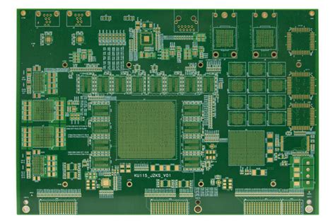
The power supply system in high-speed circuit systems can usually be divided into three physical subsystems: chip, integrated circuit packaging structure and PCB. The power grid on the chip is composed of several alternately placed metal layers. Each layer of metal consists of metal strips in the x or y direction to form a power or ground grid. Vias connect the metal strips of different layers.
For some high-performance chips, many decoupling units are integrated into the core or IO power supply. The integrated circuit packaging structure is like a reduced PCB, with several layers of complex-shaped power or ground planes. On the upper surface of the package structure, there is usually a mounting location for decoupling capacitors. PCB usually contains a continuous large-area power supply and ground plane, as well as some large and small discrete decoupling capacitor components, and a power rectifier module (VRM). Bonding wires, C4 bumps, and solder balls connect the chip, package, and PCB together.
The entire power supply system must ensure that each integrated circuit device provides a stable voltage within the normal range. However, switching currents and parasitic high-frequency effects in those power supply systems always introduce voltage noise. Its voltage change can be calculated by the following formula:
Here δv is the voltage fluctuation observed at the device and δi is the switching current. z is the input impedance observed at the device between source and ground for the entire power supply system. In order to reduce voltage fluctuations, the resistance between the power supply and ground should be kept low. In the case of DC, since z becomes a pure resistance, low resistance corresponds to low voltage drop of the power supply ir. In the case of AC, low resistance can make the transient noise generated by the switching current smaller. Of course, this requires z to be kept small over a wide frequency band.