Mastering Good PCB Design Practices for Successful Circuits
Key Takeaways
Mastering good PCB design is fundamental for anyone looking to create successful circuits. By focusing on a few key elements, you can significantly enhance both performance and reliability. First, understanding the key elements of good PCB design—like component placement, signal integrity, and grounding techniques—plays a vital role. When you plan your layout carefully, you can avoid many common pitfalls that ensnare novice designers.
Utilizing effective layout strategies can also streamline PCB manufacturing processes, minimizing the PCB manufacturing cost. For instance, maintaining adequate spacing between traces not only improves performance but aids in easier soldering during the assembly phase. If you’re new to this field and unsure of how to begin, following a step-by-step guide on designing your first PCB can be invaluable.
It is also essential to assess your designs continually. Tools for simulating PCB layouts can help you identify issues before moving on to the PCB manufacturing business stage. By actively seeking ways to improve your PCBs through iteration and feedback from PCB manufacturing companies, you increase the likelihood of a successful final product.
“Designs should not only focus on functionality but must also be ready for efficient manufacturing,” says an industry expert.
Finally, take note of case studies showcasing successful PCB designs; these lessons learned can guide your own projects towards greater success. By internalizing these practices, you’re not just improving your circuits—you’re setting yourself up for innovation in the ever-evolving world of electronics.
Introduction to PCB Design Principles
When it comes to creating efficient and reliable electronic circuits, mastering good PCB design principles is crucial. Understanding the basics of PCB manufacturing is the first step in this journey. You need to consider different aspects such as the materials used, the layout of components, and potential issues that may arise during the PCB manufacturing process. By familiarizing yourself with common challenges, you’ll be better prepared to work with PCB manufacturing companies, ensuring that your designs transition smoothly into production. Additionally, it’s vital to analyze and forecast your PCB manufacturing cost, as this will directly impact the feasibility of your projects. A well-structured PCB manufacturing business plan not only allows you to budget effectively but also gives you insight into optimizing designs for cost-efficiency without compromising quality. By combining these principles with strategic layout approaches and sound design practices, you can develop circuits that perform reliably while meeting your production requirements efficiently.
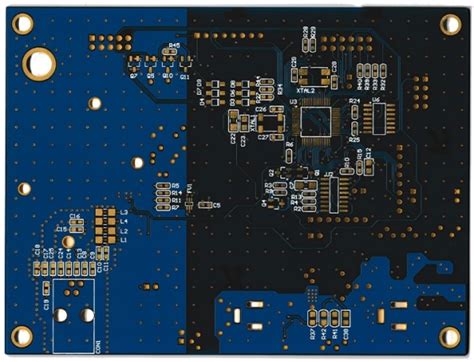
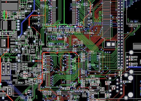
Key Elements of Good PCB Design
When embarking on the journey of PCB design, understanding the key elements is crucial for creating successful circuits. One of the fundamental aspects is ensuring optimal layout; this involves thoughtful placement of components to minimize interference and signal degradation. It’s vital to pay attention to the routing of traces as well since this directly affects both the performance and manufacturability of your design. Utilizing proper ground planes can help in managing signal integrity and noise reduction. Additionally, considering the manufacturing process during the design phase can improve your chances with various PCB manufacturing companies, as it ensures that your layout aligns with their capabilities.
Understanding the PCB manufacturing cost is also essential, as this knowledge allows you to make design decisions that keep expenses manageable without compromising quality. For instance, opting for fewer layers can reduce costs, while focusing on standard sizes can facilitate a more efficient production process. Placing a strong emphasis on design for manufacturability (DFM) principles helps bridge the gap between your creative ideas and their tangible products, leading to a smoother transition from concept to reality in your PCB manufacturing business. Ultimately, mastering these elements enhances not only your design experience but also elevates the functionality and reliability of your finished circuits, ready for implementation and scaling.
Step-by-Step Guide to Designing Your First PCB
Designing your first PCB can be both an exciting and challenging experience. To ensure a smooth journey, start by defining your project goals clearly. Understand the purpose of your PCB and its components to make informed decisions throughout the design phase. Selecting the right PCB manufacturing company is crucial, as they can significantly influence the quality and cost of your final product. Be sure to analyze pcb manufacturing costs related to different materials and features you plan to use. Once you’ve established your fundamental goals, sketch a rough layout of your board, paying close attention to component placement for optimal signal flow and minimizing interference.
Utilize specialized software tools to aid in the creation of your schematic diagrams. These tools often include libraries for standard components, streamlining the design process. After designing the schematic, you will transition into layout creation, where it’s essential to adhere to good PCB design practices that include proper trace routing, layer management, and grounding techniques. A well-thought-out layout not only ensures functionality but also prepares your design for successful pcb manufacturing.
Finally, before sending off your design for production, perform thorough checks using DRC (Design Rule Check) features in your software. This approach helps in identifying potential issues that could lead to failures or complications in the PCB manufacturing business process. Taking these steps will help you develop a robust first PCB that meets both performance criteria and production readiness standards.
Common Pitfalls in PCB Design and How to Avoid Them
In the journey toward mastering good PCB design, you’ll encounter several common pitfalls that can adversely affect your projects. One major issue stems from poor layout decisions, which often lead to signal integrity problems and increased PCB manufacturing costs. To mitigate this risk, always plan your layout carefully, keeping in mind the placement of components that require high-frequency signals. Additionally, neglecting to consider thermal management can cause components to overheat, resulting in device failure. Ensure that your design includes adequate heat dissipation features to enhance reliability.
It’s also crucial not to overlook the importance of clear documentation and communication with your chosen PCB manufacturing companies. Providing comprehensive design files and specifications can prevent misunderstandings about the intended design, which might impact both production timelines and costs. When evaluating different PCB manufacturing businesses, consider their ability to handle complex designs and maintain consistent quality within your budget constraints.
Another common oversight is disregarding design for manufacturability (DFM) principles. By integrating DFM during the early stages of your project, you can streamline production processes, potentially lowering the overall PCB manufacturing cost. Finally, always conduct thorough reviews of your designs prior to sending them for production; ensuring that all components are correctly specified will save you time and resources in the long run.
By being mindful of these pitfalls and implementing proactive strategies, you can significantly improve the effectiveness of your PCB designs and enhance their manufacturing readiness.
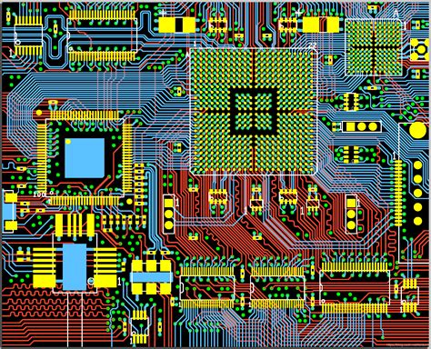
Best Practices for Effective Layout Strategies
When diving into PCB design, it’s crucial to adopt effective layout strategies that can significantly influence the performance and reliability of your circuits. Start by ensuring component placement is strategically planned; position high-frequency components close to each other to minimize signal loss and interference. It’s also essential to maintain an appropriate ground plane, as a solid ground connection is fundamental for reducing noise and improving the overall efficiency of your circuit. Furthermore, consider implementing routing techniques that prioritize short traces and minimize sharp angles; this not only ensures better signal integrity but also aids in reducing the PCB manufacturing costs by streamlining production processes.
Be mindful of your trace widths as well; inadequate width can lead to overheating or excessive voltage drop, undermining your circuit’s performance. Aim for clear labeling of traces and components, as this eases assembly and troubleshooting during the manufacturing stage. When collaborating with various PCB manufacturing companies, communicate your specific layout needs clearly; this aids in aligning design intent with manufacturing capabilities, ultimately contributing to a more efficient PCB manufacturing business process. By following these guidelines, you can significantly improve the chances that your circuits will operate seamlessly while being cost-effective during production.
Tips for Ensuring Manufacturing Readiness
Ensuring that your PCB designs are ready for manufacturing is crucial to the success of your project. To begin, it’s important to collaborate closely with PCB manufacturing companies early in the design phase. They can provide invaluable insights regarding the specific requirements necessary for efficient fabrication. Pay attention to the PCB manufacturing cost, as well—optimized designs can significantly reduce expenses and minimize production delays. Use design rules to check for clearances, traces, and components, ensuring everything adheres to standard specifications required by your chosen manufacturer. Moreover, incorporate thorough testing strategies during the design process, which will help identify potential issues before you submit your design for fabrication. One common trend is the modular approach, which streamlines changes while minimizing disruptions in production. Ultimately, investing time into these practices not only prepares your PCB for a smoother manufacturing journey but also strengthens the overall reliability of your circuits. By focusing on these areas, you contribute positively to the efficiency and success of your PCB manufacturing business.
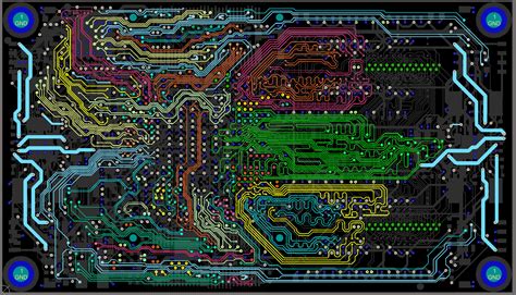
Assessing and Improving Your PCB Designs
When it comes to assessing and improving your PCB designs, the process should be both methodical and dynamic. Start by evaluating your existing layout against established benchmarks in PCB design principles. This involves scrutinizing the placement of components, traces, and vias to ensure that they align with best practices for signal integrity and thermal management. You should also consider how each element interacts with others in your circuit; sometimes what seems like a minor adjustment can significantly impact performance.
In the context of PCB manufacturing, understanding how design decisions affect the overall manufacturing cost is critical. For example, complex designs might create difficulties for PCB manufacturing companies, which could result in increased costs or longer lead times. As you assess your PCB, think about ways to streamline processes for efficient manufacturing readiness—such as reducing layer counts or selecting components that are readily available in the market.
Furthermore, don’t hesitate to make iterative improvements based on feedback from prototypes or simulation results. This not only enhances the functionality of your current designs but also lays a strong foundation for future projects within your PCB manufacturing business. Assessing and refining your PCB designs can lead to more robust circuits that are both cost-effective and easier to produce, ultimately benefiting your entire production workflow.
Case Studies: Successful PCB Designs and Lessons Learned
Learning from real-world examples enhances your understanding of good PCB design practices. By analyzing various successful PCB designs, you can identify key elements that contributed to their effectiveness. For instance, consider a case study involving a consumer electronics device that experienced challenges during the initial PCB manufacturing phases. The team recognized early on that they needed to prioritize thermal management and signal integrity to avoid issues in the final product. By consulting with reputable PCB manufacturing companies, they were able to streamline their design process. This led them to revise their layout to better accommodate pcb manufacturing cost considerations, ensuring they maintained quality while remaining budget-friendly.
Another example involved an industrial automation system where the initial designs were plagued by interference issues, jeopardizing functionality. Through comprehensive testing and engaging with experienced professionals in the pcb manufacturing business, they learned valuable lessons about component placement and grounding strategies. The end result not only improved performance but also provided insights into how to assess and iterate upon designs effectively—fostering a culture of continuous improvement within the team. Ultimately, such case studies underscore the importance of collaborating with industry experts and leveraging past learnings, allowing you to refine your own design processes while navigating the complexities of PCB projects with greater confidence.
Conclusion
In summary, mastering good PCB design practices is crucial for creating effective and reliable circuits. You should always prioritize the most critical elements such as component placement and signal routing, as they play a significant role in the overall performance of your design. Avoiding common pitfalls can save you time and reduce your PCB manufacturing cost, ensuring that you stay within your budget while achieving high-quality results. When working with PCB manufacturing companies, it’s essential to communicate clearly about your design requirements to avoid errors that could lead to increased costs or delays. By applying the best practices discussed, you can not only enhance the functionality of your circuits but also streamline the process for your PCB manufacturing business. This thoughtful approach delivers better products that meet market demands while ensuring you remain competitive in an ever-evolving industry.
FAQs
What is PCB manufacturing?
PCB manufacturing refers to the process of creating printed circuit boards that are essential for connecting electronic components in devices. This involves various stages including design, fabrication, and assembly.
What should I consider when choosing PCB manufacturing companies?
When selecting PCB manufacturing companies, consider factors such as their experience, reputation, quality control processes, and turnaround times. You should also assess their ability to handle your specific requirements, including the complexity of your design and any specialized materials you may need.
How can I estimate PCB manufacturing costs?
PCB manufacturing cost can be estimated by considering several factors such as the size of the board, the number of layers, type of materials used, and additional processes like surface mount technology. Requesting quotes from multiple manufacturers can also provide a clearer picture of potential costs.
What are common challenges in starting a PCB manufacturing business?
A few challenges in launching a PCB manufacturing business include sourcing reliable materials, adhering to strict regulatory standards, and managing production efficiency. Additionally, establishing strong relationships with suppliers and customers is crucial for success in this competitive field.
How do I ensure my PCB designs are ready for manufacturing?
To ensure your designs are manufacturing-ready, follow best practices in layout strategy and double-check all specifications for compliance with industry standards. Regular communication with PCB manufacturers during the design phase can help identify potential issues early on.