Mastering HDI PCB Design for High Density and Enhanced Performance
Key Takeaways
In your journey towards mastering HDI PCB design, understanding the nuances and advantages of high-density interconnect boards is essential. These sophisticated designs allow for greater functionality in smaller spaces, significantly impacting your pcb manufacturing processes. By focusing on optimizing board space, you not only enhance the performance of your designs but also make them more cost-effective, addressing critical aspects of pcb manufacturing cost. When considering the array of pcb manufacturing companies, selecting those with advanced techniques ensures that your project can fully leverage the benefits of HDI technology. It’s vital to keep in mind common challenges you may encounter in pcb manufacturing business, such as ensuring signal integrity and preventing issues related to electromagnetic interference. By applying advanced methodologies throughout the design and manufacturing phases, you position yourself for superior performance and reliability in any high-density solution. Remember that ongoing trends will continue to evolve, enhancing opportunities for innovation within this field, ensuring that your skills remain relevant as technology advances.
Understanding the Fundamentals of HDI PCB Design
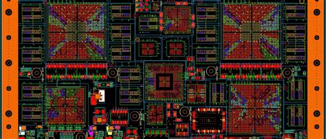
When delving into HDI PCB Design, it is essential to grasp the fundamental principles that underlie this intricate process. High-Density Interconnect boards utilize advanced techniques to create compact, high-performance circuits, making them a preferred choice in many electronic applications. One core aspect of HDI design is the elevated number of layers and vias, which facilitate greater signal routing and enhanced connectivity within a smaller footprint. This directly correlates with choices made during the PCB manufacturing phase, where careful planning can lead to optimal board space utilization. Understanding how PCB manufacturing companies integrate these elements can significantly affect the overall PCB manufacturing cost, as efficient processes lead to both reduced waste and improved quality. The landscape of the PCB manufacturing business is evolving rapidly; thus, having knowledge of these foundational concepts not only bolsters your design strategies but can also better prepare you for collaborating with industry professionals who are pivotal in delivering high-caliber HDI boards that meet or exceed performance expectations.
Key Advantages of High-Density Interconnect Boards
High-density interconnect (HDI) boards offer a plethora of benefits that are pivotal in today’s fast-paced technology landscape. For starters, HDI PCBs enable you to utilize smaller spaces effectively, making them ideal for compact devices where every millimeter counts. By integrating microvias and finer traces, you can significantly enhance the amount of circuitry within a limited footprint, ultimately allowing for the design of even smaller and more powerful electronics.
Additionally, signal integrity is markedly improved with HDI designs. The short path lengths and reduced capacitance contribute to better signal transmission, which is essential for high-speed applications. This enhancement in signal performance not only boosts the reliability of your devices but also minimizes issues related to electromagnetic interference (EMI), making your design more robust.
When it comes to cost-efficiency, while some might argue that the initial pcb manufacturing cost is higher with HDI technology due to advanced techniques and materials involved, the long-term savings from reduced sizes and improved performance can outweigh these initial investments. Engaging with reputable pcb manufacturing companies that specialize in HDI technology can further streamline this process, ensuring that your project adheres to quality standards without excessive expenditures.
As you navigate through the complexities of pcb manufacturing, consider leveraging the advanced techniques and features that HDI boards offer; not only will these augment your product’s performance but they will also position you strategically in a competitive market.
“Embracing advanced technologies like HDI is not just a trend; it’s a necessity for staying ahead.”
Here’s a simple comparison table showcasing some key advantages:
| Advantage | Traditional PCBs | HDI PCBs |
|---|---|---|
| Space Utilization | Moderate | High |
| Signal Integrity | Moderate | Superior |
| Complexity | Limited | Advanced |
| Cost Efficiency | Lower Initial Costs | Higher Initial Costs |
By adopting HDI PCB design, you empower your projects with heightened capabilities and future-ready solutions.
Techniques for Maximizing Board Space in HDI Design
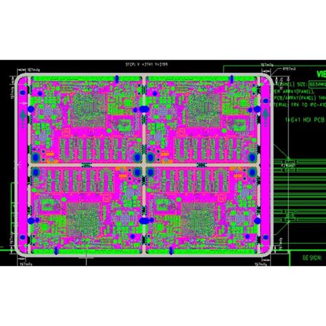
In high-density interconnect (HDI) design, maximizing board space is essential for achieving the desired functionality within a compact layout. To accomplish this, you can incorporate various strategies that enhance the efficiency of your designs. One effective approach is to utilize microvias, which are smaller than traditional vias and allow for a higher density of connections, reducing the overall footprint. Additionally, consider implementing fine-pitch components that occupy less space while providing enhanced performance. This necessitates collaboration with reputable pcb manufacturing companies that can produce these intricate designs with precision. By optimizing layer counts and strategically placing components based on signal flow, you can further minimize board size without compromising performance. Employing advanced materials and technologies in your pcb manufacturing process will also contribute significantly to decreasing the overall pcb manufacturing cost while maintaining quality standards. Ultimately, these techniques not only maximize board space but also enable more complex circuits, driving innovation in the pcb manufacturing business landscape.
Ensuring Signal Integrity in HDI PCBs
In the realm of HDI PCB design, ensuring signal integrity is paramount for achieving high performance in electronic devices. To maintain optimal signal integrity, it is crucial to consider factors such as trace width, spacing, and the overall impendance of your board. You should prioritize the use of active traces and minimize the length of connections whenever possible. Therefore, collaborating with reputable pcb manufacturing companies can significantly impact your design; they often possess advanced technologies and expertise that ensure precise routing and layering.
Additionally, proper stack-up configuration plays a vital role in maintaining signal quality. By arranging your layers effectively, you can enhance the dielectric properties and reduce electromagnetic interference significantly. When exploring options for HDI boards, it’s essential to factor in expected pcb manufacturing cost, as advanced manufacturing techniques may vary widely. Selecting a company that understands the nuances of HDI design can help mitigate costs while ensuring your project maintains its intended performance specifications.
Furthermore, using appropriate materials is crucial; for instance, high-frequency laminates can greatly enhance signal integrity at increased speeds. Ultimately, by focusing on these strategies within your design process, you can achieve superior results while also navigating the complexities of the pcb manufacturing business landscape efficiently. Ensuring robust signal integrity not only enhances device performance but also bolsters reliability in critical applications like telecommunications and high-speed computing.
Advanced Manufacturing Techniques for Enhanced HDI Performance
In the realm of HDI PCB design, understanding the advanced manufacturing techniques is essential to achieving optimal performance and high density. When you integrate innovative methods into your pcb manufacturing process, you can effectively enhance the overall quality and functionality of your boards. Techniques such as laser drilling, which allows for microvias in tighter spaces, significantly contribute to maximizing the available surface area. Moreover, ensuring precise control over the pcb manufacturing cost requires you to choose reliable pcb manufacturing companies that utilize state-of-the-art technology, promoting both efficiency and reliability. By focusing on seamless integration of layers and fine lines, you can guarantee improved signal integrity, critical in modern electronic applications. Ultimately, investing in advanced techniques not only elevates your pcb manufacturing business but also positions your designs at the forefront of technological advancement, ready to meet the demands of an ever-evolving market. As you explore these methods, you’ll discover that collaboration with expert partners can yield significant gains in performance and reliability in your HDI board designs.
Common Challenges in HDI PCB Design and Solutions
When delving into HDI PCB design, you may encounter a range of common challenges that can impact both the fabrication process and the final performance of your boards. One significant hurdle is achieving the right balance between complexity and manufacturability. As you push for higher density, the designs become more intricate, which can lead to increased PCB manufacturing costs. To mitigate this issue, it’s essential to collaborate closely with PCB manufacturing companies early in the design phase, ensuring that your innovative ideas align with their capabilities and specifications.
Another challenge is maintaining signal integrity. As the density increases and board space becomes limited, managing traces becomes critical. Using advanced techniques such as controlled impedance routing and careful attention to via placement can greatly improve performance. It is also crucial to consider the type of materials used; opting for high-frequency materials can significantly enhance your board’s reliability.
Furthermore, you’ll need to address thermal management in your designs. High-density interconnect boards tend to generate more heat due to compact layouts, which can compromise their performance if not managed correctly. Employing techniques like thermal via placement and using heat-sink solutions are effective strategies.
In conclusion, while there are notable challenges within HDI PCB design, understanding these issues allows you to implement effective solutions that not only reduce costs but also enhance overall performance. By strategically working with reputable PCB manufacturing businesses and utilizing modern techniques tailored for high-density environments, you can achieve successful outcomes without compromising on quality or integrity in your designs.
Future Trends in High-Density Interconnect Technology
As you delve into the future trends in High-Density Interconnect (HDI) technology, it’s essential to recognize the evolving landscape shaped by the demands of modern electronics. With an increased focus on miniaturization and enhanced performance, the importance of PCB manufacturing techniques becomes paramount. PCB manufacturing companies are continually innovating to develop solutions that meet these needs without sacrificing quality or reliability. Look for advancements in materials and processes that significantly reduce PCB manufacturing costs, ultimately enabling more complex designs to be realized within tight budgets.
Furthermore, trends such as automation in pcb manufacturing business processes are reshaping how boards are produced, leading to faster turnaround times and higher accuracy. This is particularly beneficial for HDI designs, where dense routing and fine pitch components challenge traditional manufacturing methods. As you explore these trends, consider how they can influence your approach to optimizing designs for signal integrity and performance. Continuous research and development in this area promise exciting opportunities to push the boundaries of what’s possible with HDI technology, enhancing everything from consumer electronics to sophisticated aerospace systems. By staying informed about these trends, you can ensure that your HDI PCB designs not only meet current specifications but are also adaptable for future advancements.
Conclusion
In summary, mastering HDI PCB design is essential for any designer aiming for advanced performance and higher efficiency. As you delve into this field, it becomes clear that the role of pcb manufacturing cannot be overstated. Choosing the right pcb manufacturing companies influences not only the quality but also the pcb manufacturing cost, which is a critical aspect of your project budget. With the increasing complexity of electronic devices, ensuring precision in pcb manufacturing business has also become paramount. You will discover that employing suitable techniques can lead to appealing outcomes while maintaining signal integrity and maximizing board space. Understanding these concepts will empower you to navigate challenges effectively and stay ahead in a rapidly evolving industry. By embracing innovative approaches, you’ll be well-equipped to push the boundaries of what is possible in high-density interconnect designs.
FAQs
What are HDI PCBs?
HDI PCBs, or High-Density Interconnect Printed Circuit Boards, are specialized boards that utilize advanced technology to achieve a denser arrangement of components compared to traditional designs. This makes them ideal for compact electronic devices.
How do HDI PCBs improve performance?
By utilizing microvias, smaller traces, and thinner substrates, HDI PCBs enhance signal integrity and reduce electromagnetic interference. This leads to better overall performance, particularly in high-frequency applications.
What challenges are associated with HDI PCB design?
Designing HDI PCBs often involves challenges such as maintaining signal integrity and managing increased manufacturing costs. Solutions can include advanced routing techniques and careful material selection to mitigate these issues.
What is the general cost of HDI PCB manufacturing?
The pcb manufacturing cost for HDI PCBs can vary widely depending on factors like layer count, complexity, and materials used. It’s advisable to consult with various pcb manufacturing companies to get accurate quotes based on your specific needs.
How can I choose the right PCB manufacturing company?
When selecting a pcb manufacturing business, consider their experience in producing HDI PCBs, the quality certifications they have, and their ability to meet your delivery timelines. Researching reviews and requesting sample works can help you make an informed decision.