Skip to content
Andwin Circuits
  • Home
  • ProductsExpand
    • HDI multilayer PCB
    • Rigid Flex PCB
    • Flex pcb
    • Special PCBExpand
      • High Frequency PCBExpand
        • Rogers RO4350B PCB
        • Rogers RO4003 pcb
        • Rogers RO3003 PCB
        • Rogers 5880 PCB
        • DICLAD 527 PCB
        • Taconic TLX series
        • Taconic TLX-8 RF PCB
        • Taconic TLX-9 RF PCB
      • High speed pcbExpand
        • Megtron 6 High Speed PCB
        • TU-872 SLK Sp High Speed
      • High TG PCBExpand
        • SHENGYI SH260 PCB
        • ISOLA 370HR PCB
        • ISOLA IS410 PCB
        • ISOLA IS420 PCB
      • Heavy copper PCB
      • Copper coin pcb
      • Copper inlay PCB
    • Metal Core PCBExpand
      • Copper core pcb
      • Aluminum PCB
      • 2 Layers Aluminum PCB
      • Direct thermal MCPCB
      • 2 Layers Direct Thermal
    • Ceramic PCBExpand
      • DPC ceramic PCB
      • DBC ceramic PCB
      • Thick film Ceramic PCB
      • Al2O3 Alumina PCB
      • AIN ALN ceramic PCB
      • IGBT Ceramic PCB
  • ServiceExpand
    • PCB Assembly
    • Quick turn PCB assembly
    • PCBA conformal coating
  • IndustryExpand
    • Telecommunication
    • IoT and Wireless
    • Industrial Control
    • Thermal management
    • Power and Energy
    • IC test board
    • Automative
    • Medical
  • CapabilityExpand
    • Rigid PCB
    • Rigid flex PCB
    • Metal core PCB
    • PCB Assembly
  • TechnologyExpand
    • Blogs
    • Via in pad
    • PCB E-test
    • PCB stack up
    • MCPCB panelization
    • Controlled impedance PCB
  • AboutExpand
    • About us
    • Certification
    • Factory Tour
  • Contact
Andwin Circuits
Home / How to make stamp hole package in PCB design

How to make stamp hole package in PCB design

ByGrace December 11, 2024December 11, 2024

1.What is stamp hole

    Stamp hole: In the motherboard assembly, the small boards need to be connected by ribs. In order to facilitate cutting, some small holes will be opened on the ribs, similar to the holes on the edge of stamps. The circular hole design similar to the segmentation in stamps has the advantages of better strength than V-Cut and can be directly broken, but the disadvantage is that the broken surface is not easy to control accurately. If the distance is too far from the line, it is easy to damage the line, which will cause scrapping.

    2.How to make stamp hole package in PCB design?

    A: Stamp hole: In the motherboard assembly, the small boards need to be connected by ribs. In order to facilitate cutting, some small holes will be opened on the ribs, similar to the holes on the edge of stamps. The circular hole design similar to the segmentation in stamps has the advantages of better strength than V-Cut and can be directly broken, but the disadvantage is that the broken surface is not easy to control accurately. If the distance is too far from the line, it is easy to damage the line, which will cause scrapping.

    Figure 4-64 Stamp hole panel

    Generally speaking, PCB panel can be made by stamp hole technology or double-sided V-groove segmentation technology. When using stamp holes, it should be noted that the overlap should be evenly distributed around each panel to avoid deformation caused by uneven force on the PCB board during welding.

    Notes on adding stamp holes:

    1) The spacing between panels is 1.6mm to 2mm, etc.

    2) Stamp holes: 8-10 0.5mm holes, hole spacing: 0.2mm, hole center distance: 1mm.

    3) Add two rows, the stamp holes extend into the board, if there are lines on the edge of the board, they need to be avoided (extending into the board: the burrs left after breaking apart do not affect the external dimensions. We often say that negative tolerance is used). After adding the stamp holes, the external shapes on both sides of the holes are connected to facilitate the subsequent work of the gong belting.

    Steps for making stamp holes:

    1) Execute the menu command “Place → Pad” to place a 0.5mm pad on the board frame line. Stamp holes are non-metallized non-plate holes, so the size of the hole and the plate are both 0.5mm, as shown in Figure 4-65. Uncheck “Plated” to make it a non-metallized hole.

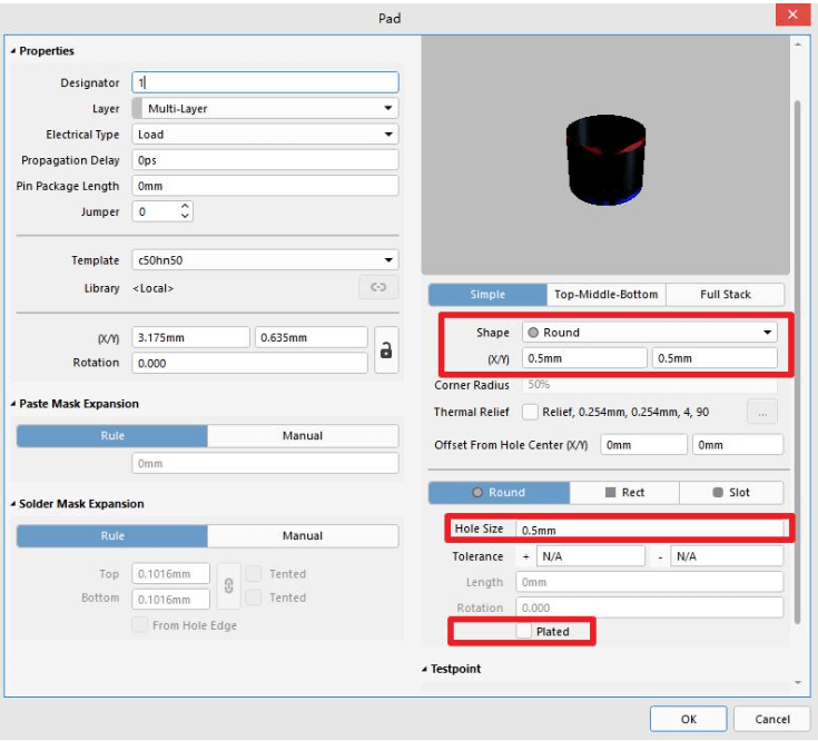
    Figure 4-65 Stamp hole attribute settings

    1) Copy the vias, use “Special Paste” to directly copy and paste the pads in the original place, with a center spacing of 1mm, and the number of copies is 4-5, and place them on both sides of the panel frame, as shown in Figure 4-66.

    2) Execute the menu command “Place → Arc → Arc (Edge)” or execute the Altium shortcut key “PAE” to quickly place the arc. The command position is shown in Figure 4-67. And click the upper and lower vias to connect the shapes on both sides of the hole. At this point, our stamp hole is complete, and the effect is shown in Figure 4-68.

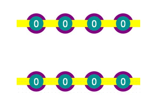
    Figure 4-66 Hole placement

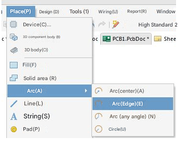
    Figure 4-67 Arc placement

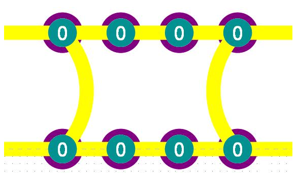
    Figure 4-68 Stamp hole panel

    3.Disadvantages of stamp holes

      ①: After the board is separated, it is saw-shaped, which some people call dog-tooth-shaped. It is easy to block the shell, and sometimes it needs to be cut off with scissors. Therefore, space should be reserved in the design process, usually by reducing the board.

      ②: Increase cost. The smallest stamp hole is 1.0MM, so this 1MM size is counted inside the board.

      4.The role of general stamp holes

        Generally, PCBs are V-CUT. Stamp holes may be used only if you encounter special-shaped or round boards. Stamp holes are used to connect boards (or empty boards), which mainly play a supporting role, and the boards will not fall apart. If the mold is opened, the mold will not collapse. . The most common use is to use them to create independent PCB modules, such as Wi-Fi, Bluetooth or core board modules, and then use them as independent components placed on another board during PCB assembly.

        5.General spacing of stamp holes

          0.55mm~~3.0mm (depending on the specific situation, commonly used 1.0mm, 1.27mm)

          Contact us for PCB quote now |

          Post Tags: #pcb design

          Post navigation

          Previous Previous
          Innovative Solutions in PCB Board Assembly for Modern Electronics
          NextContinue
          Building a Layout Inverter Using the EGS002 Driver Module

          Search

          Search

          Products

          • HDI Multilayer PCB
          • Rigid Flex PCB
          • Flex pcb
          • High Frequency PCB
          • High speed pcb
          • Heavy copper PCB
          • Metal Core PCB
          • Ceramic PCB

          Address

          Andwin Circuits Co.,Limited
          Email: sales@andwinpcb.com
          Tel: +86 755 2832 9394
          Fax:+86 755 2992  6717
          ADD:1-2F-1217,HouDeQun Industrial park,
          NanTing RD NO.56,ShaJing,BaoAn,Shenzhen 518104,GuangDong,China

          Products

          • HDI Multilayer PCB
          • Rigid Flex PCB
          • Flex pcb
          • High Frequency PCB
          • High speed pcb
          • Heavy copper PCB
          • Metal Core PCB
          • Ceramic PCB

          Technology

          • Blogs
          • Via in pad
          • PCB E-test
          • PCB stack up
          • Metal core PCB panelization
          • Controlled impedance PCB

          CERTIFICATION

          Certification >>


          Copyright© 2003 - 2026 Andwin | All Rights Reserved | Powered by Andwin

          Scroll to top
          • Home
          • Products
            • HDI multilayer PCB
            • Rigid Flex PCB
            • Flex pcb
            • Special PCB
              • High Frequency PCB
                • Rogers RO4350B PCB
                • Rogers RO4003 pcb
                • Rogers RO3003 PCB
                • Rogers 5880 PCB
                • DICLAD 527 PCB
                • Taconic TLX series
                • Taconic TLX-8 RF PCB
                • Taconic TLX-9 RF PCB
              • High speed pcb
                • Megtron 6 High Speed PCB
                • TU-872 SLK Sp High Speed
              • High TG PCB
                • SHENGYI SH260 PCB
                • ISOLA 370HR PCB
                • ISOLA IS410 PCB
                • ISOLA IS420 PCB
              • Heavy copper PCB
              • Copper coin pcb
              • Copper inlay PCB
            • Metal Core PCB
              • Copper core pcb
              • Aluminum PCB
              • 2 Layers Aluminum PCB
              • Direct thermal MCPCB
              • 2 Layers Direct Thermal
            • Ceramic PCB
              • DPC ceramic PCB
              • DBC ceramic PCB
              • Thick film Ceramic PCB
              • Al2O3 Alumina PCB
              • AIN ALN ceramic PCB
              • IGBT Ceramic PCB
          • Service
            • PCB Assembly
            • Quick turn PCB assembly
            • PCBA conformal coating
          • Industry
            • Telecommunication
            • IoT and Wireless
            • Industrial Control
            • Thermal management
            • Power and Energy
            • IC test board
            • Automative
            • Medical
          • Capability
            • Rigid PCB
            • Rigid flex PCB
            • Metal core PCB
            • PCB Assembly
          • Technology
            • Blogs
            • Via in pad
            • PCB E-test
            • PCB stack up
            • MCPCB panelization
            • Controlled impedance PCB
          • About
            • About us
            • Certification
            • Factory Tour
          • Contact
          Search