Circuit board chewed by rats
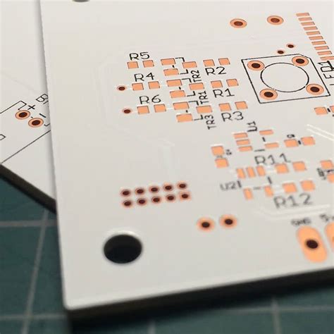
Mice are small and delicate. Once they bite anything, they will leave their tiny teeth marks as evidence. Sometimes you will find these tiny teeth marks on your circuit board. But don’t be afraid, these teeth marks don’t mean you may be infected with germs spread by mice.
In fact, these tiny holes can help you separate the circuit board from the whole production board. The position and size of the holes are very precise. Of course, it does look like the mouse teeth marks left on those mouse-bitten objects.
Therefore, you don’t have to prepare cheese and mouse traps to lure those mice running around. The mouse teeth marks on the PCB board discussed in this article have nothing to do with real mice. Instead, we will focus on the PCB mouse teeth holes and the corresponding sizes to ensure that you have a deeper understanding of the PCB production process and circuit boards.
01 What is a mouse bite hole?
A mouse bite hole (Mouse bite) on a circuit board is a part of the PCB production board that is used to aggregate small PCBs to facilitate the production process. In addition, some people use mouse bit
e marks to describe the phenomenon of excessive corrosion of the copper on the PCB (etching gap). This is not what the rat tooth mark in this article means.
PCB manufacturers use CAM software to combine PCB circuit boards into a large production board. In order to be able to fix the production board in the later production process, the assembler and manufacturer need to provide additional board space outside the PCB circuit, which is especially important for small circuit boards.
Usually, the boards in the production process have a uniform size, so you can lay out multiple PCB circuit board patterns on a standard board. This not only makes the production process easier, but more importantly, it reduces the production cost. The production cost of producing multiple boards is the same as that of one board.
1.1 Production PCB splicing boards Once the production is completed, just as you put them together into a large layout before, you need to separate them again. This process is called depanelization. Depanelization can be done using V-grooves, pre-scored lines, or direct cutting. You need to pre-score these grooves on the edges of the separators to facilitate separation, or to separate the circuit board from the fixed edge board. These board edges used for fixing in the production process are called “breakout tabs”.
For easy separation, dense holes are usually arranged in a line. When the circuit board is broken off from the fixed edge, dense rat teeth marks will be left. You can polish them smooth later.
02 Position and size
The small holes used for separation are of various types, but most manufacturers use five closely spaced small holes for board separation. The diameter of the separation holes is 0.5mm (0.020inch). As for the spacing, most of them are 0.76mm (0.03inch).
The space and size of the separation holes on the PCB board appear random, which reduces the cleaning work after separation. The smaller the holes, the easier it is to clean after separation, but more drilling processes are required during processing, and more materials will be saved.
If the diameter of the separation hole is too large, it will be difficult to clean the edge after separation. The position of the separation holes on the PCB board is also important. An important principle is that they are as close to the edge of the PCB as possible, so that there will be less PCB board waste after separation.
2.1 Four PCBs in one
◎ Fixed border placement conditions
The following factors need to be considered when placing fixed borders around the planned circuit board:
In order to prevent the milling cutter from being worn, overused, and saving time, do not prevent too many fixed borders around the circuit board;
The fixed borders need to be sufficient to support the circuit to complete the entire production process;
The fixed borders should be at least 0.125 inches (3.2mm) away from the components closest to the circuit board;
Do not place fixed borders around the circuit or sensitive devices, which will cause these locations to suffer more stress during the separation process;
The damage caused to the circuit by the application of the fixed border peeling process may not be discovered immediately, and sometimes it will cause intermittent circuit failures, making the troubleshooting process extremely difficult. This is why it is necessary to keep the fixed borders away from the circuit board to improve the circuit yield rate.
Of course, if the fixed borders are placed too few, it will not be able to support the circuit board to complete the entire production process. The bending and deformation of the circuit board will cause the assembly process to be unreliable. At this time, the experience and knowledge of making PCBs will come in handy.
03 V-grooves on PCB
In order to separate the circuit board, it is often necessary to carve a V-groove on the circuit board with a milling cutter, that is, to cut off some material in the thickness direction of the PCB board, leaving a small part to connect the circuit boards together. In the final stage of production, the milling cutter mills the V-groove outline on the PCB, and then cuts them off from the production circuit board. This can be done with a special V-groove cutter. Here are some guidelines for V-grooves:
◎ V-groove placement guidelines
Make sure the gap between the boards is 0mm, that is, each board is directly connected, and there is no spare board to be removed;
The center line of the V-groove needs to be 0.35mm away from the outer contour of the board;
The V-groove needs to be straight, vertical or horizontal;
The size of the PCCB with the V-groove must be at least 75mm×75mm, and the maximum size must not exceed 450mm×1245mm;
04 Separating boards
Generally, there are three types of methods for separating the boards integrated on a PCB panel:
◎ Label card
In this case, some unnecessary PCB parts need to be cut off from the circuit in advance, leaving only separation holes to connect the sub-boards. They can be connected to each other for easy subsequent generation, and it is also easy to manually break them apart.
◎ V-groove
This is the most common method for separating boards. Mill a V-groove around each separate board. For thick boards, the groove depth reaches one-third of the board thickness. Usually the grooves are symmetrically carved on the top and bottom of the circuit board.
◎ Direct cutting
In this case, there are no rat-tooth holes or V-shaped grooves between the sub-modules on the entire circuit board. So how to separate the circuit boards? Two methods are often used:
For circuit boards with a thickness of less than 1mm, laser cutting can be used. This method is costly and the cutting process will also generate vibration and dust.
Using a curved bow tool or a rotary tool for cutting, this processing technology is cheap and not very efficient.
Compared with the previous two methods, this cutting method is rarely used now.
For most applications, using label cards and V-shaped grooves to separate the sub-circuits on the normal production board is the most commonly used. For PCB designers, they need to understand which method is better for their application, and then determine how to aggregate the circuit boards into normal production boards to ensure that the separation process is easier and has high support strength.
05 Label card and V-shaped groove
How to choose to use label card or V-shaped groove to separate circuit boards during the circuit board production process. Here are some factors to consider:
◎ Edge components
When designing a label card separation solution, it is necessary to consider that the separation point should not be too close to the edge components of the circuit board. This can be avoided by changing the position. If a V-groove is used, it is only necessary to ensure that the separation groove is not too close to the outermost components of the circuit board.
◎ Circuit board shape
If the circuit board is in a regular rectangular shape, the separation solution using a V-groove is more suitable. When the circuit board is irregular in shape, it is better to use a label type, that is, to use rat teeth holes to separate the circuit board.
◎ Time factor
The processing time of the discrete solution using a label card is long, while the processing time of a V-groove is short.
◎ Edge quality
If you have high requirements for the edge quality of the circuit board after separation, it is better to use a label card. After separation, only a small rat tooth mark will remain on the edge of the circuit board, which can be removed by local grinding with sandpaper. The entire edge of the circuit board separated by the V-groove appears rough, and more post-grinding is required to improve the edge quality of the circuit board.
◎ Material utilization rate
The V-groove separation solution has the highest utilization rate for PCB boards. Label cards will waste a certain amount of PCB boards, which will increase the cost of PCB production.