Comprehensive PCB Design and Manufacturing Services Explained
Key Takeaways
Understanding the PCB design and manufacturing landscape is crucial for professionals and hobbyists working in electronics. A well-executed pcb assembly process ensures that the final product meets both performance and quality standards. The design phase involves several key steps, including schematic capture, layout design, and component selection that together will dictate the effectiveness of the assembled circuit board. Recognizing how pcba integrates with manufacturing processes helps in selecting the right materials and fabrication techniques, ultimately leading to higher efficiency and reliability. Moreover, as industry standards evolve, staying informed about the latest technologies in PCB manufacturing is essential—options such as automated assembly lines and advanced testing methods are revolutionizing production capabilities. Understanding best practices for high-quality PCB production can minimize errors and enhance functionality across various applications—from consumer electronics to aerospace components. As challenges continue to arise in this dynamic field, key stakeholders must adopt creative approaches to navigate issues effectively while maintaining a focus on quality assurance. Overall, these insights lay a foundation for thriving in the intricate world of PCB services while ensuring optimal performance in every project undertaken.

Introduction to PCB Design and Manufacturing
Printed Circuit Boards (PCBs) are essential components in electronic devices, serving as the backbone for electrical connections. The process of PCB design involves intricate planning and execution that balances functionality, manufacturability, and reliability. It begins with the creation of schematic diagrams, which are essential to define the electrical connections between different components. Once the design is established, it progresses to layout development where considerations such as trace width, layer stack-up, and component placement become critical.
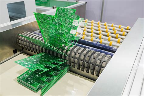
Manufacturing these boards requires specialized equipment and knowledge. Utilization of advanced technologies such as automated pcb assembly (PCBA) systems optimizes production efficiency while ensuring high precision. The technology can automate component placement, soldering, and inspection processes—thereby reducing human error and enhancing the overall quality of the boards produced.
The integration of quality control throughout manufacturing is vital. Implementing techniques such as design for manufacturability (DFM) ensures that design choices do not hinder production capabilities or lead to costly errors. By adopting best practices in both design and manufacturing stages, organizations can produce robust PCBs tailored for a range of applications from consumer electronics to industrial machinery.
Here’s a brief overview highlighting key aspects of PCB design and manufacturing:
| Aspect | Description |
|---|---|
| Design Tools | Software used for creating PCB layouts |
| Manufacturing Techniques | Processes like soldering, etching, and drilling |
| Quality Assurance | Ensures boards meet established electrical standards |
| Testing Methods | Techniques like functional testing to validate performance |
In summary, understanding the relationship between PCB design processes and manufacturing technologies is crucial for anyone involved in electronics today. Mastery over these processes directly influences not only functionality but also the long-term reliability of electronic products in an increasingly demanding market.
Understanding PCB Design Process: Key Steps and Considerations
The PCB design process is a meticulous journey that requires a blend of creativity and engineering expertise. It begins with defining the circuit requirements, including functionality, power consumption, and interconnectivity. Once the specifications are clear, designers create a schematic diagram that serves as a roadmap for the layout. The subsequent step involves translating this schematic into a physical layout using specialized software, which creates the visual representation of how the printed circuit board (PCB) will look. Key considerations during this phase include component placement, trace routing, and ensuring proper spacing to minimize electromagnetic interference (EMI).
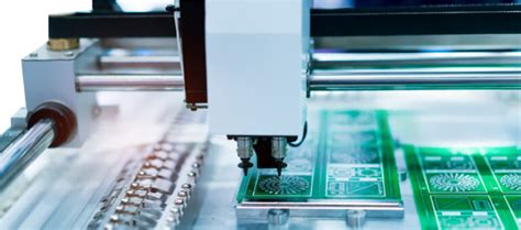
After drafting the layout, designers perform comprehensive simulations to detect potential issues before actual production. This is where technologies such as Computer-Aided Design (CAD) play an essential role in validating electrical integrity. Once optimizations are made, the design moves to the manufacturing stage where PCB assembly (commonly referred to as PCBA) takes place. Here, components are soldered onto the PCB according to industry standards. Attention to detail during this stage is crucial for ensuring durability and performance in various applications.
Overall, understanding each step of the PCB design process not only enhances the quality of PCBA but also enables designers to create highly functioning circuit boards tailored for specific needs in diverse industries. With careful planning and execution, professionals can ensure reliability and efficiency in their designs while adhering to best practices within PCB manufacturing services.
Latest Technologies in PCB Manufacturing
The landscape of PCB manufacturing has witnessed significant advancements, greatly enhancing the efficiency and quality of pcb assembly processes. Modern technologies such as Surface Mount Technology (SMT) and automated optical inspection (AOI) play a crucial role in streamlining production. By allowing for miniaturization of circuit designs, SMT enables the placement of components directly onto board surfaces, optimizing space and performance. Moreover, AOI systems contribute to quality assurance by identifying defects and ensuring that each PCBA meets stringent specifications before it reaches the final assembly stage.
Another revolutionary development is the use of 3D printing in prototyping and production. This method allows for rapid iteration, which is particularly valuable during the design process as it facilitates quick modifications to circuit layouts without extensive delays. Additionally, printed electronics—a subtype of 3D printing—are becoming increasingly popular due to their ability to integrate electronic functionality directly into flexible substrates.
“Embracing new technologies not only improves efficiency but also reduces costs associated with traditional manufacturing processes.”
Furthermore, Internet of Things (IoT) integration is reshaping PCB designs, enabling smart devices to become more interconnected and capable. As such, the demand for high-density interconnections is increasing, leading manufacturers to adopt microvias and advanced materials that enhance electrical performance while maintaining mechanical reliability.
These innovations represent just a fraction of what’s possible in PCB manufacturing today. Adopting these latest technologies results in more reliable products that can withstand the test of time—a critical consideration for any professional or enthusiast involved in electronic design and production.

Best Practices for High-Quality PCB Production
To achieve high-quality PCB production, it is essential to adhere to a set of best practices that encompass every stage of the design and manufacturing process. One of the primary considerations is meticulous pcb assembly planning. Ensuring that components are placed accurately and optimally is crucial for maintaining functionality and reliability. Additionally, the selection of suitable materials cannot be overlooked; using high-grade substrates ensures durability and performance under various conditions.
Furthermore, implementing rigorous testing methods throughout the production cycle can significantly reduce the risk of defects. Regular inspections, including Automated Optical Inspection (AOI) and functional testing post-pcba, can catch issues early, saving time and costs in the long run. Collaboration among design engineers and manufacturing teams fosters a culture of quality, facilitating prompt identification and resolution of potential problems.
Lastly, investing in the latest technologies—such as advanced CAD software for design simulations—enables clearer insights into potential challenges before physical production begins. By incorporating these best practices, manufacturers can produce PCBs that meet or exceed industry standards, ensuring reliability across various applications. Ultimately, a commitment to continuous improvement in these areas will significantly enhance the quality and functionality of PCB assembly services offered in the marketplace.
Common Applications for PCB Designs
Printed Circuit Boards (PCBs) serve as the backbone of modern electronics, with applications spanning numerous industries. From consumer electronics like smartphones and laptops to automotive systems that ensure the functionality of safety features and infotainment systems, the role of PCB assembly in these devices is crucial. In the medical field, advanced PCBA technology is employed to create reliable devices such as heart monitors and diagnostic equipment that require high precision and durability. Furthermore, in industrial automation, complex PCB designs facilitate efficient control systems, while telecommunications heavily rely on sophisticated boards for reliable data transmission. The aerospace sector also incorporates specialized PCBs that endure extreme conditions, ensuring the integrity of vital systems during flight. As these applications evolve, embracing innovative technologies in design and manufacturing becomes increasingly important to meet rigorous performance demands and enhance functionality across diverse sectors. The significance of high-quality PCB manufacturing services cannot be overstated, as they directly impact device reliability and efficiency across these various applications.
Challenges in PCB Manufacturing and How to Overcome Them
The challenges in PCB manufacturing are multifaceted, often encompassing issues related to materials, design intricacies, and production techniques. One of the primary obstacles is ensuring high-quality materials are consistently sourced. Inferior materials can lead to failures in the finished product, which is particularly critical when dealing with applications requiring rigorous reliability, such as in telecommunications or medical devices. To address this, engaging reputable suppliers who can provide certified materials is essential.
Another significant challenge is the intricacy of the design process itself. As complexity increases with designs that integrate more advanced functionalities, the potential for errors also rises. This can result in manufacturing delays or faulty PCB assembly. To mitigate these risks, employing state-of-the-art design software and conducting thorough design reviews before moving to production can greatly enhance accuracy and alignment with specifications.
Furthermore, as electronic devices become more compact and feature-rich, manufacturers are pressured to produce denser boards while maintaining proper signal integrity and thermal management. Employing advanced technologies such as multi-layer boards and utilizing precise PCBA techniques can significantly contribute to overcoming these limitations.
Lastly, staying ahead of evolving industry standards and customer requirements poses an ongoing challenge. Continuous education within teams about best practices in both design and manufacturing processes ensures adaptability to new trends. Regular training sessions focused on quality assurance protocols will also empower personnel to identify potential issues early on. By proactively addressing these challenges through strategic planning and technology adoption, companies can not only improve their PCB manufacturing services but also enhance overall product reliability in a competitive marketplace.
Future Trends in PCB Design and Manufacturing
As the technology landscape evolves, the future trends in PCB design and manufacturing are becoming increasingly centered around sustainability, automation, and advanced materials. One of the most notable trends is the shift towards green manufacturing practices that focus on reducing waste and minimizing environmental impact through the use of recyclable materials. This pushes manufacturers to rethink their processes to develop more efficient pcb assembly techniques that incorporate eco-friendly methods.
Moreover, advancements in automation are significantly influencing the speed and accuracy of PCBA (Printed Circuit Board Assembly). Automated production lines are being integrated with smart technologies such as AI and machine learning, allowing for real-time monitoring and adjustments, which not only enhance quality control but also reduce production costs.
In addition, emerging materials such as flexible PCBs and high-frequency interfaces are opening new doors for innovation. These materials facilitate the design of more compact and lightweight devices without compromising on performance, which is essential for a multitude of applications ranging from consumer electronics to sophisticated communication systems.
Ultimately, these trends illustrate a clear shift towards more efficient, sustainable, and technologically advanced solutions in PCB design and manufacturing, establishing a foundation for future developments that will continue to shape our increasingly connected world. As these changes take root, professionals in the field must stay abreast of these innovations to ensure their designs meet both current demands and future expectations.
Conclusion: The Importance of Quality in PCB Services
In the realm of PCB design and manufacturing, the emphasis on quality cannot be overstated. The intricacies involved in developing a Printed Circuit Board (PCB) necessitate adherence to stringent standards and protocols throughout the pcb assembly process. High-quality pcba not only ensures improved functionality and reliability of electronic devices but also significantly impacts the overall performance of integrated systems. Investing in superior PCB manufacturing services allows businesses to mitigate risks associated with operational failures and costly downtime typically linked to inferior components. Additionally, meticulous attention to detail during the design phase is essential to achieve optimal layout and routing, which directly affects signal integrity and electrical performance. As industries continue to evolve, the demand for high-quality circuit boards will remain pivotal; hence, professionals must prioritize excellence in every aspect of PCB production. Ultimately, committing to top-tier practices in PCB services will not only enhance product durability but also foster innovation across various applications, solidifying a company’s reputation in a competitive market.
Conclusion: The Importance of Quality in PCB Services
In today’s rapidly evolving technology landscape, the significance of high-quality PCB design and manufacturing services cannot be overstated. As various industries increasingly rely on Printed Circuit Boards (PCBs) for their products, ensuring that these components meet stringent quality standards is imperative. Quality in PCB assembly ensures not only the functionality but also the longevity of electronic devices. By leveraging advanced technologies, such as automated assembly and precision engineering, manufacturers can enhance the reliability of their PCBA processes. Furthermore, adhering to best practices during production minimizes common defects and maximizes performance. Ultimately, professionals and enthusiasts must prioritize quality in every stage of PCB development—from initial design through to the final assembly—to achieve optimal results in their applications. This commitment to quality service fosters innovation and drives success across various sectors that depend on reliable electronic components.
FAQs
What is PCB assembly?
PCB assembly, often referred to as PCBA, is the process of soldering electronic components onto a printed circuit board (PCB) to create functional devices. This step transforms a bare PCB into a completed circuit board, ready for use in various electronic applications.
Why is the quality of PCB assembly important?
The quality of PCB assembly affects the durability and performance of the end product. High-quality PCBA ensures reliable connections, reduces the risk of failure, and enhances the overall functionality of the electronic device.
What are the common technologies used in PCB assembly?
Common technologies in PCBA include surface mount technology (SMT) and through-hole technology. SMT allows for smaller components to be placed directly onto the surface of the PCB, while through-hole involves inserting leads into pre-drilled holes. Both methods have their advantages depending on the application’s requirements.
How can I ensure high-quality PCB assembly?
Ensuring high-quality PCB assembly involves following best practices such as using reliable materials, maintaining precise alignment during placement, employing experienced technicians, and conducting thorough testing at various stages of production. Quality control measures play a crucial role in this process.
What are some typical applications for PCBs?
PCBs are used in numerous applications ranging from consumer electronics like smartphones and laptops to industrial machinery, medical devices, automotive systems, and telecommunications equipment. The versatility of PCBs makes them a fundamental component in virtually all electronics.