Innovations in Multi Layer PCB Assembly Techniques for Efficiency
Key Takeaways
In the realm of multi-layer PCB assembly, the integration of advanced materials and innovative techniques is crucial for enhancing production efficiency. As the demand for compact and high-performance electronic devices grows, manufacturers are challenged to optimize their pcba processes. The emergence of automated solutions and robotics in pcb assembly not only increases output but also ensures precision in intricate designs. By adopting advanced manufacturing strategies, companies can significantly reduce lead times while improving overall quality. It’s essential to recognize that fostering continuous improvement through the analysis of production data can pinpoint inefficiencies, driving further innovations in the industry. Ultimately, these evolving methodologies are set to redefine best practices within multi-layer PCBs, paving the way for a more efficient future in electronics manufacturing.
Introduction to Multi-Layer PCB Assembly
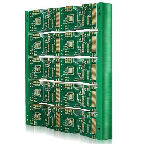
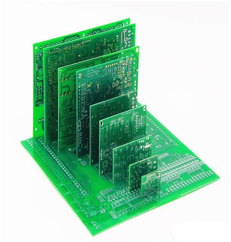
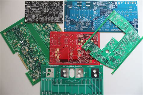
The realm of multi-layer PCB assembly (commonly referred to as PCBA) plays a pivotal role in modern electronics, enabling the integration of complex circuits into compact designs. As technology advances, the demand for efficient and reliable pcb assembly processes has surged. Innovations in materials and techniques have led to significant improvements in production efficiency, reducing costs and lead times. For instance, the use of high-frequency substrates and flexible materials has revolutionized traditional assembly methods, allowing for greater design flexibility and performance optimization. Moreover, the implementation of automated processes has streamlined workflows, minimizing human error and enhancing precision during assembly.
One essential aspect of pcb assembly is the layering technique itself, wherein multiple layers are intricately combined to create complex circuit designs. This not only conserves space but also allows for better thermal management and signal integrity within electronic devices. Clearly outlined methodologies in multi-layer PCB assembly emphasize not only reliability but also scalability, catering to various industry demands.
In addition to robust design practices, emerging technologies such as machine learning and data analytics are now being leveraged to improve defect detection rates and overall quality assurance during production. The convergence of these technologies marks a transformative era for PCBA, where efficiency is paramount amidst ever-increasing consumer expectations.
| Innovation Area | Impact on Production Efficiency |
|---|---|
| High-Frequency Substrates | Enhanced signal integrity |
| Flexible Materials | Increased design adaptability |
| Automation Technologies | Reduced production time |
| Machine Learning Algorithms | Improved quality control |
In summary, understanding the intricacies of multi-layer PCB assembly is essential for manufacturers striving to enhance their operational efficiency while maintaining high standards in product development. With ongoing advancements in both materials and processes, the future looks bright for innovation within pcb assembly, paving the way for more sophisticated electronic applications.
Current Challenges in PCB Assembly Efficiency
The landscape of PCB assembly is continually evolving, yet several challenges hinder optimal efficiency. One significant issue is the increasing complexity of printed circuit boards (PCBs), particularly in multi-layer PCB assembly. As the demand for advanced features grows, manufacturers face difficulties in maintaining quality while implementing effective assembly processes. The intricacy of designs often leads to longer production times and higher rates of defectivity.
Moreover, sourcing high-quality materials that align with both performance and cost-effectiveness remains a pressing concern. Many manufacturers struggle to balance the need for innovation with the availability and affordability of advanced materials necessary for producing reliable PCBA. Additionally, supply chain disruptions can impact timely access to essential components, further complicating production schedules.
“To navigate these challenges effectively, embracing technological advancements and fostering supplier relationships is crucial for ensuring a smooth assembly process.”
Another challenge stems from implementing automation into PCB assembly processes. While automation has proven beneficial for reducing labor costs and improving precision, many firms encounter barriers such as integrating new systems with existing workflows and ensuring that staff are adequately trained to operate sophisticated machinery.
Ultimately, addressing these hurdles requires a strategic approach that combines innovation with practical solutions to enhance the efficiency of multi-layer PCB assembly while ensuring high standards in quality control. The future of the electronics manufacturing industry depends on overcoming these challenges through resilient practices and continuous adaptation to evolving demands.
Advanced Materials Transforming Multi-Layer PCBs
The evolution of multi-layer PCB assembly has been significantly influenced by the introduction of advanced materials that enhance both performance and production efficiency. High-frequency materials, such as Gallium Arsenide (GaAs) and low-loss dielectrics, are now commonly used to improve signal integrity in increasingly complex designs. Additionally, the integration of flexible substrates allows for pcb assembly in applications requiring tighter spaces without sacrificing functionality. Not only do these materials support higher component density, but they also contribute to reduced weight and improved thermal management in various devices. Furthermore, innovations such as lead-free solder and advanced laminates ensure compatibility with emerging environmental standards while maintaining the durability of the assembled boards. This shift towards utilizing these sophisticated materials not only optimizes the manufacturing process but also drives future advancements in the pcba domain, ultimately fostering a more sustainable electronics industry.
Innovative Techniques for Enhanced Production
The landscape of pcb assembly has evolved significantly with the introduction of innovative techniques aimed at enhancing production efficiency. One noteworthy approach is the integration of advanced materials that not only improve the performance of multi-layer PCBs but also streamline the manufacturing process. These materials facilitate better signal integrity and thermal management, which can lead to reduced weight and size in electronic devices, ultimately pushing the boundaries of what is possible in compact design. Furthermore, the adoption of precision assembly technologies, such as automated optical inspection (AOI) systems, has drastically improved accuracy and consistency in pcba processes. Such innovations minimize human error and allow manufacturers to maintain high standards even with complex board layouts. In addition to materials and inspection technologies, implementing a modular design approach can further enhance production efficiency by allowing for quicker reconfiguration during the assembly process. This flexibility enables companies to adapt swiftly to market demands while maintaining a high throughput in their operations. Overall, these innovative techniques play a crucial role in redefining pcb assembly, driving efficiencies that benefit both manufacturers and consumers alike.
Automation and Robotics in PCB Assembly Processes
The integration of automation and robotics in PCB assembly processes is revolutionizing the electronics manufacturing landscape. By implementing advanced robotic systems, manufacturers can enhance the precision and speed of their PCBA operations. These systems facilitate the handling of complex multi-layer PCBs, reducing human error and increasing overall production efficiency. For instance, automated pick-and-place machines can precisely position components on a PCB, ensuring accurate alignment that is crucial for device performance. Additionally, robotic arms equipped with vision systems can monitor assembly quality in real time, allowing for immediate corrections if discrepancies are detected. As these technologies continue to evolve, they not only improve output but also reduce operational costs by minimizing waste and maximizing resource utilization in the manufacturing process. The results are clear: automation and robotics are essential drivers of innovation, ultimately enhancing both the quality and efficiency of multi-layer PCB assembly operations.
Case Studies: Success Stories in Efficiency
In the evolving landscape of PCB assembly, several companies have made significant strides in enhancing pcba production efficiency through innovative practices. One notable example is a leading electronics manufacturer that adopted advanced surface mount technology, allowing for tighter component placement and reduced cycle times. By implementing automated testing and inspection processes, this company minimized defects and increased yield rates, demonstrating the importance of quality assurance in multi-layer PCB assembly. Another case study highlights a firm that integrated robotic pick-and-place systems into their assembly line, resulting in a remarkable decrease in labor costs while improving precision and throughput. The use of advanced materials, such as high-density interconnect substrates, not only supported these innovations but also encouraged miniaturization of devices, aligning with the growing demand for compact electronics. Through these real-world examples, it becomes clear that embracing innovation in pcb assembly processes can lead to substantial benefits, setting a precedent for future practices in the electronic manufacturing industry.
Future Trends in Multi-Layer PCB Manufacturing
As the electronics industry continues to evolve, the multi-layer PCB assembly processes are witnessing transformative changes aimed at enhancing efficiency and effectiveness. One of the most notable trends is the adoption of high-density interconnects (HDI), which allows for increased functionality without expanding the board size. This not only optimizes space but also improves electrical performance, making it a key player in modern PCBA techniques. Additionally, there is a growing emphasis on sustainable practices, prompting manufacturers to explore eco-friendly materials and processes in pcb assembly. The integration of automated systems is becoming more prevalent, significantly reducing human error and accelerating production times while maintaining high-quality standards. Furthermore, advancements in software for design simulation and manufacturing execution systems (MES) are enhancing decision-making capabilities within production environments. These technologies facilitate data-driven insights that are crucial for continuous improvement in multi-layer PCB assembly lines. With these innovations at the forefront, companies that leverage them can expect substantial gains in productivity and reduced operational costs, positioning themselves competitively in an ever-expanding market.
Conclusion: The Impact of Innovations on the Industry
The advent of innovative techniques in multi-layer PCB assembly has significantly transformed the landscape of PCB assembly processes within the electronics manufacturing sector. As industries continue to adopt more complex and compact designs, advancements in materials and technologies have become essential. For instance, the integration of advanced materials not only improves performance but also facilitates better thermal management, which is critical in high-density applications. Moreover, the implementation of automation and robotics in PCBA processes drives consistency and precision, reducing defects that were previously common in manual operations. These innovations not only enhance production speed but also increase cost-efficiency, enabling manufacturers to keep pace with market demands while maintaining high-quality standards. Looking ahead, it is clear that as these technologies continue to evolve and mature, they will further reshape strategies within the industry, positioning companies to respond deftly to emerging trends and consumer expectations. The proactive stance on embracing innovation ensures that businesses remain competitive and capable of delivering sophisticated electronic solutions effectively.
Conclusion: The Impact of Innovations on the Industry
As we have explored throughout this article, advancements in multi-layer PCB assembly techniques are reshaping the landscape of electronics manufacturing. The integration of innovative materials and the adoption of automation are key components driving greater efficiency in the PCB assembly process. Techniques such as automated optical inspections and laser direct imaging have provided manufacturers with tools that not only improve precision but also reduce production time, ultimately contributing to a more streamlined workflow. The use of advanced PCBA methods enables manufacturers to manage complexities and mitigate common issues associated with multilayer constructions, thus ensuring quality and reliability in end products. Moreover, real-world case studies highlight how companies leveraging these innovations have seen improved turnaround times and reduced costs, affirming the significant impact these techniques have had on production metrics. As we move forward, keeping an eye on future trends will be essential for industries aiming to stay competitive in a rapidly evolving market, ultimately making pcb assembly more efficient and sustainable.
FAQs
What is multi-layer PCB assembly?
Multi-layer PCB assembly refers to the process of creating printed circuit boards that consist of multiple layers of circuitry. This design allows for greater complexity and functionality in a compact space, often used in advanced electronic devices.
What are the advantages of multi-layer PCBs in electronics?
The primary advantages include improved performance, reduced signal interference, and the ability to incorporate more components than single-layer boards. Multi-layer PCBA enables more complex circuit designs, making them ideal for high-density applications.
How do advanced materials impact multi-layer PCB assembly?
Advanced materials enhance the durability and reliability of pcba processes. For instance, high-frequency laminates can improve signal integrity, while thermal management materials ensure adequate heat dissipation.
What innovative techniques are being used for enhanced production efficiency?
Innovative techniques such as advanced automated assembly systems and improved soldering methods are being utilized to increase production speed and accuracy. Techniques like selective soldering and laser soldering have shown promise in optimizing effectiveness.
How is automation transforming PCB assembly processes?
Automation increases precision while reducing human error in pcb assembly, leading to lower production costs and shorter lead times. Robotics can perform repetitive tasks at high speed, creating a more efficient workflow.
Can you provide examples of successful case studies in multi-layer PCB efficiency?
Several electronics manufacturers have successfully implemented new techniques that resulted in significant reductions in assembly time and cost. These case studies showcase the transformative impact of innovations within the industry.