Are FPGAs the new PCBs?
Perhaps the biggest change in the industry in recent years has been the introduction of low-cost microprocessors. Microprocessors were first used to implement calculators and then personal computers. With their dynamic reconfiguration capabilities, they have replaced many hard-wired digital system circuits, bringing true “embedded artificial intelligence” to previously “dumb” devices.
The key to the success of the microprocessor is not the device itself, but the ability it gives engineers to move important design challenges from a hard-wired environment to the “soft” realm. Board-level hardware platform design continues to use the familiar “hard-wired, off-the-shelf device” model, but the development of product features or intelligence in the platform can be added as “software.” With this platform-based approach, the risk of manufacturing the same physical hardware is greatly reduced because the features can be modified after the hardware is built.
Originally developed as an efficient and upgradeable tool, the microprocessor has finally rewritten the rules of electronics. It is no longer enough to be cheap, reliable, and work efficiently, now electronics needs to be “smart.”
With the microprocessor having changed the face of electronic design over the past decade, it is clear that FPGAs represent the next “big thing” in the industry.
Due to the large capacity, high performance, and relatively low cost of FPGAs, previously fixed design elements (such as processors and their peripheral devices and logic blocks) can be moved to a soft domain. This is so attractive because it has the potential to bring the same level of freedom to hardware design that the shift of functionality to software brought to developers as microprocessors became widely available.
The programmable nature of FPGAs is a boon to development, allowing hardware designs to be modified without the time and cost penalties inherent in re-manufacturing boards. And the underlying system hardware can be modified immediately after the product is shipped or in production. The high-level treatment enjoyed by the software side of the development process can now be extended to the hardware, so that the configurable intelligence of the product is not only in the software, but also in the soft-wired circuits implemented in the FPGA.
With the microprocessor having changed the face of electronic design in the past decade, FPGAs clearly represent the next “big thing” in the industry.
The question is, if designers do not have the expertise required for current FPGA design, how can they avoid being shut out of the paradigm shift in electronic design?
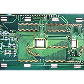
Until recently, FPGA design has been largely owned and operated by HDL experts. Traditional FPGA design techniques have evolved from the perspective of defining device functionality. FPGA developers define the logic functions of the FPGA at the register transfer level (RTL) using hardware description languages such as Verilog and VHDL. Because FPGA real estate was relatively expensive in the past, the focus was on abstracting n levels of optimization from a given programmable device.
With the reduction in the price of high-volume programmable devices, these devices may be used as complete system platforms, which greatly changes people’s above-mentioned views. Defining the logic functions of the device RTL requires developing FPGA functions at a higher level of abstraction. The focus on system-level design has made mainstream system engineers happy to join the FPGA club, who may not be HDL or FPGA design experts.

Back to the Future
From a device perspective, the purpose of this stage is to achieve large-scale adoption of FPGAs as system development platforms. However, the current reliance on HDL methods limits the large number of engineers who can easily work in this field. In particular, from a tool perspective, what is needed is an FPGA design method that can provide a high level of abstraction, but can be used by most engineers who are engaged in system design. While searching around for methods, it is worth revisiting the mainstay of today’s industry – board-level design technology. Board-level embedded system engineers routinely create designs that effectively contain millions of basic gates. However, they do not need to deal with the complexity of register-level or gate-level design; the system complexity is contained in the devices used to build the circuits. Designers only use these large, off-the-shelf devices and treat them as “black boxes” during system development.
While large IP devices are available for FPGAs, the IP blocks and devices are primarily HDL source files. FPGA designers must instantiate the IP in the target source code, which often requires knowledge of how the logic blocks are assembled. Once included in the circuit description, the entire system (including the large IP blocks) must be synthesized for the target device.
Current FPGA IP distribution methods tend to increase rather than reduce the complexity of the FPGA design process and are far from being ready for use.
Clearly, for system-level design in FPGAs to be efficient and usable by mainstream engineers, the IP delivered for FPGA implementation must be streamlined and made “usable.” Furthermore, the design environment for using this IP must have the same flexibility and high level of abstraction that designers enjoy in board-level systems.
Successful Devices
Altium, a leading provider of electronic product development solutions, has taken up this challenge with its latest release of the Altium Designer system. Altium Designer seeks to combine board-level and FPGA-level system design to create an integrated digital system development solution, allowing board-level designers to create FPGA systems using the tools and skills of building board-based implementation systems.
Altium’s approach is to package the functionality required to build soft systems into large soft devices and provide designers with an environment to assemble the devices using a familiar schematic approach. The design can then be automatically implemented on the target FPGA device.
FPGA-based devices with pre-synthesized models are supplied as schematic symbols, and each device is synthesized for a range of target FPGAs. During the design process, the correct model for the selected target device is automatically abstracted and sent to the FPGA synthesis engine along with the connection information defined in the schematic to be processed as a “black box factory”.
The result is that systems for FPGA implementation can be created in Altium Designer in the same way that systems for board implementation are created – FPGA devices are taken from a library, placed on a schematic and connected together to form the system hardware. Altium’s classic board-level design system, Protel, is actually a license option for Altium Designer with an input environment that has been enhanced to include FPGA development capabilities.

Test Time
Equally important as inputting a system is the ability to test and debug the system during development. Traditional FPGA design flows rely heavily on HDL-level simulation to resolve potential timing and functional issues.
This is because the functional blocks that make up the circuit are instantiated as source code and the entire system must be synthesized for implementation, which can cause problems even in previously tested code blocks. The larger and more complex the system, the more difficult and time-consuming the simulation process becomes. In fact, in many FPGA applications, simulation can take as much time as the primary design process.
Board-level simulation plays a supporting role in the actual testing of circuit hardware verification. Because the devices used to build the circuit are assumed to operate within the manufacturer’s specifications, there is no need to verify the performance of the device itself.